- 易迪拓培训,专注于微波、射频、天线设计工程师的培养
Microchip MCP3903三相电表六路模拟前端解决方案
录入:edatop.com 点击:
Microchip公司的MCP3903是业界首个用于三相电表的六路模拟前端(AFE),包括三对两个带PGA同步取样Delta-Sigma的16/24位ADC,相位延迟补偿区块,基准电压以及SPI兼容的高速10MHz串行接口.转换器中的抖动算法能降低闲音(idle tones),改善THD,SINAD为91dB,THD为-100dBc,SFDR为102dB,可编程数据速率高达64ksps,关断模式功耗小于2uA,任意两路间串扰为-115dB,内部基准电源的温票为5 ppm/°C,主要用在电表和能量测量,手提仪表以及医疗和电源监视等.本文介绍了MCP3903主要特性,功能方框图以及用于16位MCU的MCP3903 ADC评估板亮点,电路图和材料清单与PCB元件布局图.
Microchips First Six-Channel Analog Front End for Three-Phase Energy Metering Offers Industry-Leading Accuracy Microchip
The MCP3903 is a six-channel Analog Front End (AFE) containing three pairs made out of two synchronous sampling Delta-Sigma Analog-to-Digital Converters (ADC) with PGA, a phase delay compensation block, internal voltage reference, and high-speed 10 MHz SPI compatible serial interface. The converters contain a proprietary dithering algorithm for reduced idle tones and improved THD.
The internal register map contains 24-bit wide ADC data words, a modulator output register as well as six 24-bit writable control registers to program gain, over-sampling ratio, phase, resolution, dithering, shut-down, reset and several communication features.
The communication is largely simplified with various Continuous Read modes that can be accessed by the Direct Memory Access (DMA) of an MCU and with separate Data Ready pins that can directly be connected to the Interrupt Request (IRQ) input of an MCU. The MCP3903 is capable of interfacing to a large variety of voltage and current sensors including shunts, current transformers, Rogowski coils, and Hall-effect Sensors.
MCP3903主要特性:
• Six Synchronous Sampling 16/24-bit Resolution Delta-Sigma A/D Converters with Proprietary Multi-Bit Architecture
• 91 dB SINAD, -100 dBc Total Harmonic Distortion (THD) (up to 35th harmonic), 102 dB Spurious-free Dynamic Range (SFDR) for Each Channel
• Programmable Data Rate up to 64 ksps
• Ultra Low-Power Shutdown Mode with <2 μA
• -115 dB Crosstalk Between any Two Channels
• Low Drift Internal Voltage Reference: 5 ppm/°C
• Differential Voltage Reference Input Pins
• High Gain PGA on Each Channel (up to 32 V/V)
• Phase Delay Compensation Between Each Pair of Channels with 1 μs Time Resolution
• High-Speed Addressable 10 MHz SPI Interface with Mode 0,0 and 1,1 Compatibility
• Independent Analog and Digital Power Supplies 4.5V - 5.5V AVDD, 2.7V - 3.6V DVDD
• Available in Small 28-lead SSOP Package
• Extended Temperature Range: -40°C to +125°C
MCP3903应用:
• Energy Metering and Power Measurement
• Portable Instrumentation
• Medical and Power Monitoring
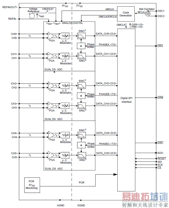
图1.MCP3903功能方框图
用于16位MCU的MCP3903 ADC评估板
The MCP3903 ADC Evaluation Board for 16-Bit MCUs system lets users evaluate the performance of the MCP3903 six-channel ADC. It also provides a development platform for 16-bit PIC® MCU-based applications, using existing 100-pin PIM systems, compatible with the Explorer-16 and other high pincount PIC demo boards. The system comes with programmed PIC24FJ128GA010 PIM modules that communicate with the LabView GUI for data exchange and ADC setup.
MCP3903 ADC评估板亮点:
• Six-channel ADC MCP3903 output display using serial communication to the PC Software Interface and LCD
• Simultaneous 4 ksps at 91 dB Signal-to-Noise and Distortion Ratio (SINAD) performance. The ADC can run up to 64 ksps.
• System and ADC performance analysis through graphical PC tools showing Time domain scope plot, Frequency Domain (FFT), and statistical numerical analysis.
• Robust hardware design with analog grounding and analog/digital separation, allowing low noise evaluation of the MCP3903 devices. Separate power supplies and power planes - 4 layer board.
• Pigtail Plus connectors for Explorer-16 daughter board compatibility.
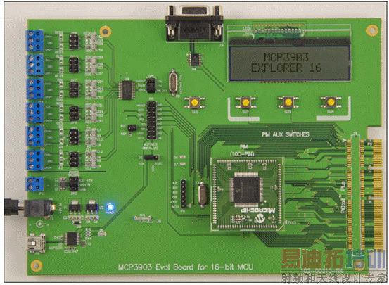
图2.MCP3903 ADC评估板外形图
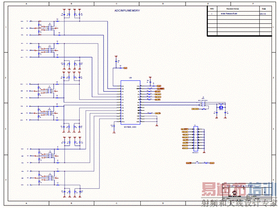
图3.MCP3903 ADC评估板电路图(1):模拟
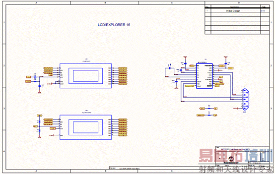
图4.MCP3903 ADC评估板电路图(2) CD和UART
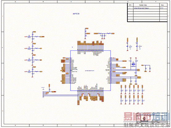
图5.MCP3903 ADC评估板电路图(3):USB和存储器

图6.MCP3903 ADC评估板电路图(4):MCU
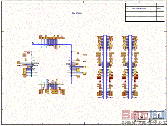
图7.MCP3903 ADC评估板电路图(4) IM模块
IM模块
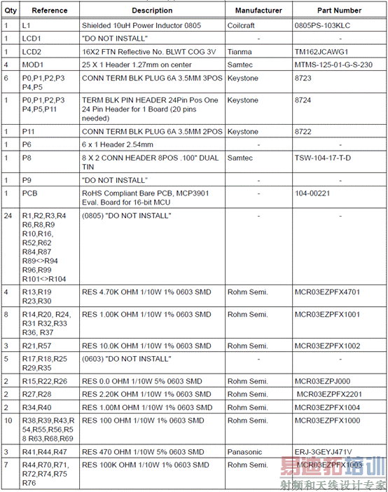
图8.MCP3903 ADC评估板电路图(5):电源
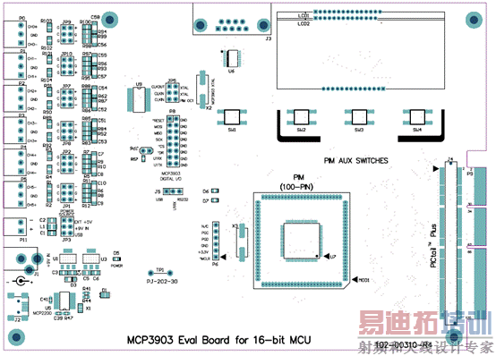
图9.MCP3903 ADC评估板元件布局图:正面
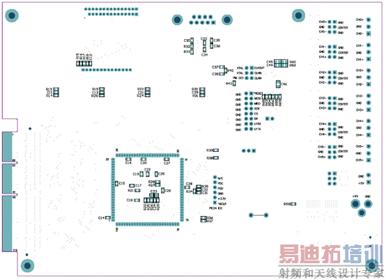
图10.MCP3903 ADC评估板元件布局图:背面
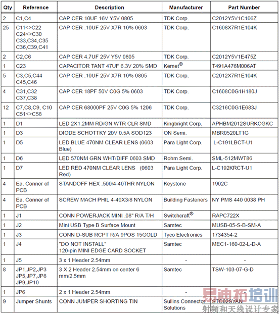
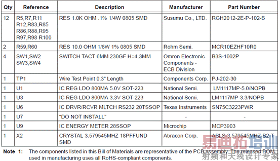
MCP3903 ADC评估板材料清单:

详情请见:
http://ww1.microchip.com/downloads/en/DeviceDoc/25048B.pdf
和
http://ww1.microchip.com/downloads/en/DeviceDoc/51994A.pdf
Microchips First Six-Channel Analog Front End for Three-Phase Energy Metering Offers Industry-Leading Accuracy Microchip
The MCP3903 is a six-channel Analog Front End (AFE) containing three pairs made out of two synchronous sampling Delta-Sigma Analog-to-Digital Converters (ADC) with PGA, a phase delay compensation block, internal voltage reference, and high-speed 10 MHz SPI compatible serial interface. The converters contain a proprietary dithering algorithm for reduced idle tones and improved THD.
The internal register map contains 24-bit wide ADC data words, a modulator output register as well as six 24-bit writable control registers to program gain, over-sampling ratio, phase, resolution, dithering, shut-down, reset and several communication features.
The communication is largely simplified with various Continuous Read modes that can be accessed by the Direct Memory Access (DMA) of an MCU and with separate Data Ready pins that can directly be connected to the Interrupt Request (IRQ) input of an MCU. The MCP3903 is capable of interfacing to a large variety of voltage and current sensors including shunts, current transformers, Rogowski coils, and Hall-effect Sensors.
MCP3903主要特性:
• Six Synchronous Sampling 16/24-bit Resolution Delta-Sigma A/D Converters with Proprietary Multi-Bit Architecture
• 91 dB SINAD, -100 dBc Total Harmonic Distortion (THD) (up to 35th harmonic), 102 dB Spurious-free Dynamic Range (SFDR) for Each Channel
• Programmable Data Rate up to 64 ksps
• Ultra Low-Power Shutdown Mode with <2 μA
• -115 dB Crosstalk Between any Two Channels
• Low Drift Internal Voltage Reference: 5 ppm/°C
• Differential Voltage Reference Input Pins
• High Gain PGA on Each Channel (up to 32 V/V)
• Phase Delay Compensation Between Each Pair of Channels with 1 μs Time Resolution
• High-Speed Addressable 10 MHz SPI Interface with Mode 0,0 and 1,1 Compatibility
• Independent Analog and Digital Power Supplies 4.5V - 5.5V AVDD, 2.7V - 3.6V DVDD
• Available in Small 28-lead SSOP Package
• Extended Temperature Range: -40°C to +125°C
MCP3903应用:
• Energy Metering and Power Measurement
• Portable Instrumentation
• Medical and Power Monitoring

图1.MCP3903功能方框图
用于16位MCU的MCP3903 ADC评估板
The MCP3903 ADC Evaluation Board for 16-Bit MCUs system lets users evaluate the performance of the MCP3903 six-channel ADC. It also provides a development platform for 16-bit PIC® MCU-based applications, using existing 100-pin PIM systems, compatible with the Explorer-16 and other high pincount PIC demo boards. The system comes with programmed PIC24FJ128GA010 PIM modules that communicate with the LabView GUI for data exchange and ADC setup.
MCP3903 ADC评估板亮点:
• Six-channel ADC MCP3903 output display using serial communication to the PC Software Interface and LCD
• Simultaneous 4 ksps at 91 dB Signal-to-Noise and Distortion Ratio (SINAD) performance. The ADC can run up to 64 ksps.
• System and ADC performance analysis through graphical PC tools showing Time domain scope plot, Frequency Domain (FFT), and statistical numerical analysis.
• Robust hardware design with analog grounding and analog/digital separation, allowing low noise evaluation of the MCP3903 devices. Separate power supplies and power planes - 4 layer board.
• Pigtail Plus connectors for Explorer-16 daughter board compatibility.

图2.MCP3903 ADC评估板外形图

图3.MCP3903 ADC评估板电路图(1):模拟

图4.MCP3903 ADC评估板电路图(2)
 CD和UART
图5.MCP3903 ADC评估板电路图(3):USB和存储器

图6.MCP3903 ADC评估板电路图(4):MCU

图7.MCP3903 ADC评估板电路图(4)
 IM模块
IM模块
图8.MCP3903 ADC评估板电路图(5):电源

图9.MCP3903 ADC评估板元件布局图:正面

图10.MCP3903 ADC评估板元件布局图:背面
MCP3903 ADC评估板材料清单:


详情请见:
http://ww1.microchip.com/downloads/en/DeviceDoc/25048B.pdf
和
http://ww1.microchip.com/downloads/en/DeviceDoc/51994A.pdf


