关于AGC指数函数产生电路的疑惑
录入:edatop.com 阅读:
最近看了一篇关于AGC指数函数产生电路的论文,a low power monolithic AGC with automatic DC offset cancellation for direct conversion hybrid CDMA transceiver used in telemetering。对文中关于指数函数产生电路有一点疑惑。
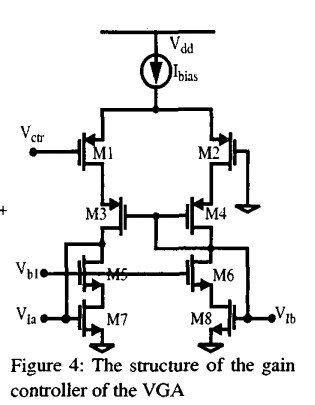
文中VGA的指数函数产生电路如下图所示:

关于这个电路的描述是这样的:The biasing currents of the VGA are varied by a simple gain controller, Fig.4. The controller is mainly composed of a differential pair. The currents, which flow in two current sources - M7&8, are controlled by M1&2. M3&4 are added to improve the VGA‘s gain in decibels which changes more linearly with the control voltage(Fig.5). The gate of M1&2 are connected to Vctr and ground respectively. By varying the Vctr from 0V to 1.5V, the gain of the VGA sweeps from minimum to maximum(Fig.5).
不知道这个电路的指数表达式是如何推导出来的?求高手解释
文中VGA的指数函数产生电路如下图所示:

关于这个电路的描述是这样的:The biasing currents of the VGA are varied by a simple gain controller, Fig.4. The controller is mainly composed of a differential pair. The currents, which flow in two current sources - M7&8, are controlled by M1&2. M3&4 are added to improve the VGA‘s gain in decibels which changes more linearly with the control voltage(Fig.5). The gate of M1&2 are connected to Vctr and ground respectively. By varying the Vctr from 0V to 1.5V, the gain of the VGA sweeps from minimum to maximum(Fig.5).
不知道这个电路的指数表达式是如何推导出来的?求高手解释
[attach]587305[/attach]
顶一下,求高手回答
帮顶,同问
再顶一个
申明:网友回复良莠不齐,仅供参考。如需专业解答,请学习本站推出的微波射频专业培训课程。
上一篇:没外部电源也能正常工作,你敢信!
下一篇:USB2.0数据线上加保护-电容限制求助

