关于CCO

各位:
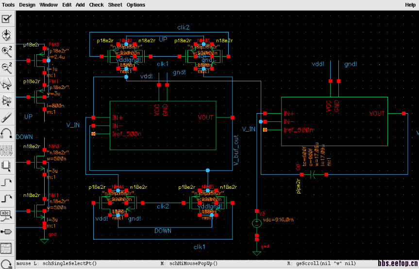
最近在做一个CCO,以上是CCO的部分电路截图,其中左边的四个管子为镜像电流源(电流源未画出),PM0和PM1、NM0和NM1分别为用来为电容放电、充电的电流支路,中间为一个缓冲器以及四个CMOS开关(由互补开关控制),最右边为运放和电容构成的积分器。进行tran分析时积分器的输出直接上拉到vdd了,积分器的反相输入端输出锯齿波(而且会拉到0电位后在上升)。请问:积分器的反相输入端是不应该是虚地点啊?还有,电容在直流时是开路的,积分器的运放如何实现反馈的啊?谢谢!
thanks dear , so much
请问阁下可以指点一下吗?
Could you translate it to EN ?
everybody: Above is CCO of the partial circuit of shots, the left of the four tubes for the mirror current source (not shown) current source, PM0, PM1, NM0 and NM1 respectively used for the capacitive discharge, charging current branch in the middle of a buffer and four CMOS switch (controlled by a complementary switching), and the rightmost the op amp and a capacitor of the integrator. Tran analysis directly on the output of the integrator when pulled vdd, the inverting input terminal of the integrator output sawtooth (and will be pulled to zero potential after the rise). The problem is: the inverting input of the integrator should not be a virtual location? There, the capacitance in DC is open, how to achieve feedback op amp integrator? Thank you
申明:网友回复良莠不齐,仅供参考。如需专业解答,请学习本站推出的微波射频专业培训课程。

