You can ignore the glitch-impulse area that occurs at the output of DACs during code transition in most systems. However, in a control loop, this DAC idiosyncrasy may have a negative effect. You would think that a transition from one bit to the next with a DAC would go smoothly. After all, the voltage-out difference of two consecutive codes from a DAC is equivalent to a mere least-significant bit.
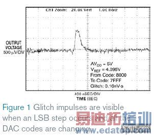
The glitch-impulse area occurs during the DAC’s output-voltage-transition region as it switches from one code to another. A 16-bit DAC code transition from 8001h to 8000h produces an imperceptible glitch at the voltage-output terminal because few switches are internally changing in the DAC. If the same 16-bit DAC switches from 8000h to 7FFFh, or half the full-scale output voltage, the output-glitch impulse becomes noticeable to the extent that it appears as if the DAC is momentarily nonmonotonic. Secondary glitches occur around one-fourth full-scale and three-fourths full-scale voltages.

shows an example of the output-glitch impulse with a major code transition at half the full-scale of a 16-bit DAC.
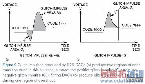
DAC glitches are a product of capacitive-charge injection from the internal gates and asynchronous gate switching. The DAC glitch manifests itself with two lobes

if there is charge injection across the parasitic capacitance of the switching gates. Typically, R2R-ladder DACs have a two-lobe glitch impulse. A second type of glitch is the single-lobe glitch impulse

. A single-lobe glitch, which DACs with a string topology usually produce, results from asynchronous switching of several internal DAC gates.
In control systems, the DAC glitch impulse from major code transitions confuses the loop by momentarily sending an erroneous output-voltage signal. If the control system is fast enough to respond to this glitch, the circuit may oscillate. You can try to reduce the impact of this glitch impulse by using a lowpass filter at the output of the DAC. However, although a lowpass filter reduces the glitch impulse amplitude, it increases the glitch time. For example, the glitch-impulse response of the 16-bit DAC in

is equal to 96 nV-sec, with peak voltage of 75 mV and duration of 1.6 祍ec. You can filter this glitch impulse so that the peak voltage is 37.5 mV, but the duration of the glitch impulse is now 3.2 祍ec. You can also implement sampling circuitry on the output of the DAC, timing it with DAC conversions. This technique may work for lower-resolution DACs; however, the sampling mechanism may create more problems by adding analog errors and conversion time. The best way to overcome larger glitch impulses is to select a string-DAC with lower glitch-impulse errors from the start.
