- 易迪拓培训,专注于微波、射频、天线设计工程师的培养
使用线性充电器实现强大可靠的系统设计(英)
- Protection against transient voltage spikes
- Unregulated adaptor output voltage characteristics
- Thermal management and fault protection
This article discusses the system level impact of these parameters when using a wide range of AC adaptors and how a robust system can be designed using a linear charger with features like over voltage protection, thermal regulation and dynamic timers. It also references the TI bq2406X series as an example of a family of linear chargers designed specifically to address the above mentioned concerns.
Wide variety of AC adaptors
One of the main aspects of portable systems designed today is the requirement to accept a wide range of input power sources like AC adaptor, USB cable or a car/airplane DC outlet. The wide success of rechargeable portable equipment has seen numerous vendors developing after market adaptors at a fraction of the price as an alternative to expensive original equipment manufacturer (OEM) adaptors. The most popular of these sources, the AC adaptor, in general can be characterized into two groups: regulated adaptors, typically OEM adaptors; and unregulated adaptors, typically aftermarket adaptors.
The regulated adaptor output voltage has internal circuits that provide very good line and load regulation. Unregulated adaptors, on the other hand, provide an output voltage that is dependent on the load, and have poor line regulation. The adaptor behavior under over-current conditions is also different. Regulated adaptors usually have a more abrupt transition region when entering an over-current region, as shown in Figure 1.
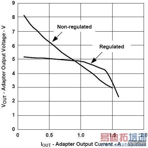
Figure 1: Regulated and Un-regulated AC adaptor characteristics
Input transient and over voltage conditions
Modern day portable equipment that is designed to be powered from the above discussed types of adaptors must incorporate protection functions that minimize risks of end equipment damage caused by over voltage conditions. Over voltage conditions can be categorized into two modes: a DC over voltage and a transient over voltage.
Usually, a DC over voltage is caused by plugging in an aftermarket or non-standard adaptor with an incorrect output voltage. On the other hand, a transient over voltage occurs when an adaptor is hot-plugged into the end equipment. The transient over voltage can easily approach 2x the nominal adaptor output voltage as shown in Figure 2.
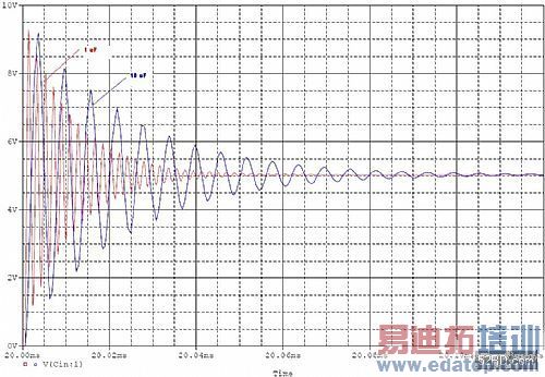
Figure 2: Adaptor hot plug transient behavior for a 5V, 1A adaptor with 1uF and 10uf input capacitor
The charger stage, if properly designed, may be used to isolate the external power supply from the battery and the system as shown in Figure 3. In this topology, the positive terminal of the battery pack and the system are connected to the output of the charger. The charger power stage effectively isolates the external adaptor from the system power bus.
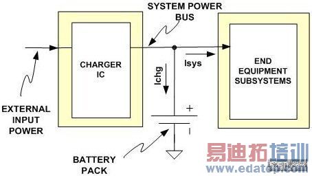
Figure 3: A charger stage isolates external power supply from the battery and system
A robust design is achieved when the topology shown in Figure 3 is implemented and an input over voltage protection (OVP) function is incorporated in the charger stage to monitor the input voltage and disable the charger power stage if a DC over voltage condition is detected. When the charger stage is disabled the system power bus is completely isolated from the adaptor output. The Input OVP threshold is usually set at 6.5V for a 5V regulated adaptor. The bq2406X family offers options of 6.5V and 10.5V to accommodate both regulated and unregulated adaptors.
To isolate and protect the system and battery from external supply transient over voltage conditions, a charger stage with a wide input voltage rating of approximately 2X the rating of the nominal adaptor voltage can be used.
It is to be noted that in the above discussed topology a potential lock up condition can develop if the minimal system current (in stand-by mode, for instance) exceeds the termination current threshold. If the system current exceeds the termination threshold, termination is never detected. The safety timer is activated, powering down the charger stage before the battery is charged to full capacity. To solve this potential problem, the bq2406X family provides an option to disable the safety timer and charge termination functions when the equipment is in high power mode while the battery charger in enabled.
Thermal management and fault protectionA high input to system power bus voltage differential in a linear charger can cause the die temperature to rise beyond maximum junction temperature value and cause thermal damage. To avoid this problem, a robust thermal management scheme needs be considered for such designs that include both thermal shutdown and thermal regulation.
As a general rule all integrated charger ICs must have an internal thermal shutdown that is triggered once the IC internal junction temperature exceeds a maximum junction temperature value in order to ensure that no thermal damage occurs during operation. In a typical application, thermal shutdown will be activated when the charger input voltage is above the battery voltage by 2-3V for charge currents in the order of 1A. When activated, the thermal shutdown circuit will turn off the charger power stage to avoid thermal damage. Usually thermal shutdown circuits have a hysteresis by design. When the IC die temperature decreases the power stage is turned back on. The die temperature will increase until the thermal shutdown circuit is activated again. The thermal constants can be in the order of seconds, depending on the PCB layout, and this mode of operation can generate a "flashing" pattern on the charge status LEDs.
To deal with this thermal problem a thermal loop can be added, reducing the charge current to keep the IC junction temperature below the thermal shutdown threshold. The operation of a thermal loop added to bq2406x family of linear chargers is shown in Figure 3. The thermal loop effectively reduces the charge current when activated, decreasing the power dissipation in the charger stage power MOSFET.
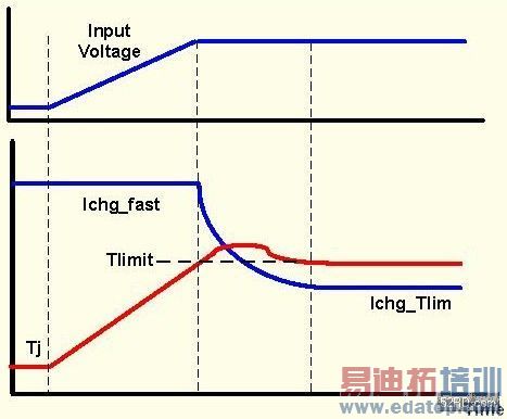
Figure 4: Thermal loop operation during input voltage transient
It should be noted that in linear chargers with thermal loops, the charge current can be reduced to very low values if the input voltage is too high. Under these conditions a false termination can be detected if the charge current falls below the termination threshold. To avoid this problem, bq2406X disables termination when the thermal loop is active.
Dynamic timer control
The charge safety timer is set to detect a fault condition if the charge cycle duration exceeds the total time expected under normal conditions with the charge current equal to the fast charge current rate. When the thermal loop is activated, the charge current is reduced. Now a false safety timer fault can be observed if the thermal loop is active for a long period of time. To avoid this undesirable fault condition, the bq2406X Charger IC activates the dynamic timer control (DTC), an internal circuit that slows down the safety timer clock effectively adding an extra time to the programmed timeout value. The DTC circuit is enabled whenever the thermal loop is active.
The thermal regulation function in conjunction with the DTC circuit provides a robust thermal management and fault protection scheme to protect the charger stage and system from thermal faults caused by transient or other overvoltage conditions.
Conclusion
Portable devices are here to stay and the competition is fierce among manufacturers to innovate and differentiate. The end users will continue to challenge the robustness and stability of the portable equipment by putting them through harsh environments like leaving the phone to charge in the car on a hot summer day or plugging in an inexpensive aftermarket or a wrong adaptor. A key differentiator of one product from the other is its stability, reliability and robustness under these undesirable conditions. The onus is on the system design engineer to take these factors into consideration to make his product smarter, stronger and robust enough to standout as "The" one in a million and not "A" one in a million.

