- 易迪拓培训,专注于微波、射频、天线设计工程师的培养
平板音频设计以平面屏幕展现跌宕起伏的音频(英)
HDTV audio transmissions are a compressed digital signal, so newer TVs tend to use a digital path, keeping the audio signal 100 percent digital from the RF transmitter to the speaker. The analog signal is more susceptible to noise, so it must be routed carefully, run differentially or shielded to avoid degradation, whereas the digital signal has a high tolerance to noise. Most TV sound processors have both analog and digital outputs, so this is generally not an issue. The analog-based system would not need an ADC to mux in auxiliary inputs. Muxing in the digital domain is very simple, if signals are already digital.
Adding effects, like speaker equalization, midnight mode or third party algorithms like SRS TruSurround, is much simpler in the digital domain. With the digital signal path this can even be done as the final step on the production line, enabling a single PCB to be used across many platforms.
Design Issues
Designing audio amplifiers for flat panel TVs involves several challenging and juxtaposed issues. Engineering is usually fraught with making trade-offs and there’s no better example than in flat panel design. How does one design a 20 watt (W) stereo audio amp in a slim-line DLP, plasma or Liquid Crystal Display (LCD) chassis and still dissipate the heat generated? How does one support the 2-layer, size-constrained board space and still meet the electromagnetic interference (EMI) testing requirements? How does one cost effectively design printed circuit boards (PCBs) for various screen sizes and power levels and still meet tight deadlines?
Fortunately, engineers do not need to tackle these obstacles by themselves. Many of these challenges have been overcome or workarounds have been developed. New devices are now available to help solve these issues through integrating functionality. One way to address these challenges and speed design time is with the latest Texas Instruments audio class-D amplifier product offerings, the TPA3100D2 and TPA3101D2.
The TPA3100D2 and TPA3101D2 are stereo class-D amplifiers designed for the flat panel market. They are pin-for-pin compatible and drive stereo 20W and 10W, respectively. New integrated features include improved pop/click control, adaptive dynamic range control and enhancements to reduce EMI. These products overcome issues in previous class-D generation devices and speed the design process.
Output Wattage
The first consideration in an audio amplifier design is to determine the output wattage needed. This is directly proportional to screen size as explained below. Other factors to consider are speaker impedance, Total Harmonic Distortion (THD), amplifier voltage and amplifier efficiency. All these factors are interrelated. For example, higher speaker impedance gives better efficiency and thermal performance, but requires a higher amplifier voltage or produces clipping at a lower output power. Understanding the trade-offs in these factors and achieving a balance is the key to a good design.
The TPA3100D2 is highly efficient -- capable of 92 percent efficiency at full output power, 20Wx2. At this efficiency, 1.74W needs to be dissipated at full power. This power is easily dissipated from the package by soldering the thermal pad on the bottom of the package to the PCB. A ground plane in the PCB serves as the heat sink, eliminating the need for an external heat sink. These properties make the TPA3100D2 ideal for flat panel Plasma and LCD TVs greater than 32 inches in size. These televisions require higher audio power, because the end user is seated further away from the speakers.
The TPA3101D2 is a cost-effective 10Wx2 solution for smaller LCD televisions ranging from 23 to 32 inches wide. The TPA3101D2 is a pin-to-pin compatible device to the TPA3100D2 with all the same features. The efficiency is 87 percent for 10Wx2.
Because the TPA3100D2 and TPA3101D2 have exactly the same pin-out, package dimensions and external components, this allows the same board design to be used for different products -- saving design and manufacturing time and inventory costs.
Thermal Performance and Maximum Output Power
Thermal performance is another important consideration when designing audio solutions for TVs. Heat dissipation is a critical issue in flat panel TVs. Too much heat build-up can distort the colors of an LCD screen, but over-design can inflate the build of materials (BOM) cost. In addition, as a class-D amplifier heats up, it becomes less efficient and will output less audio power. It is critical that the thermal considerations be taken into account early in the design process.
Different thermal conditions and requirements can impact the maximum output power of the TPA3100D2 and TPA3101D2. The following explains the factors involved and presents a systematic method to determine the device maximum output power. Note that the information is a theoretical estimation; actual thermal measurements are still required.
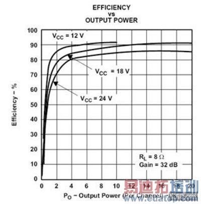
Figure 1: TPA3100D2 Efficiency versus Output Power Graph
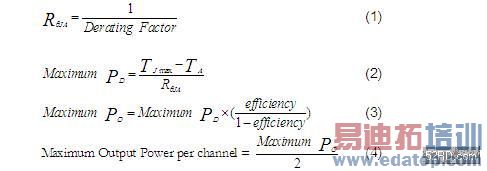
If your internal specification requires the case temperature to remain below a given temperature, assume TCmax is slightly less than TJmax. A good rule-of-thumb is to assume TJmax is 10 oC higher than TCmax. The calculations can be re-run to maintain the case temperature within specification.
Using the above method, TPA3100D2 at VCC=18V, RL=8, TA=55 oC and TJmax=150 oC, we obtain a maximum output power of 20W per channel.
If we increase the ambient temperature to 65 oC, the maximum output power will be reduced to 18W per channel.
EMI is electromagnetic radiation, which is emitted by electrical circuits carrying rapidly changing signals, such as the outputs of a class-D audio power amplifier. EMI must be below limits set by regulatory standards such as CISPR 22 or FCC Part 15 Class B. TI’s class-D amplifiers have proprietary, integrated circuitry to control EMI.
Some class-D amplifiers use a technique called "spread-spectrum," which claims to reduce EMI. This technique randomly changes the fundamental switching frequency of the class-D amplifier and "spreads" the EMI over a frequency band. TI’s amplifiers do not include this feature as this technique raises the noise floor by 6 dB and does not lower the EMI peaks significantly. EMI requirements can be better met by good board layout practices and minimizing current loops. This results in a 6 dB improvement of signal-to-noise ratio (SNR) to the listener.
TI class-D amplifiers use a modulation scheme called "BD" modulation (see www.ti.com/bd for more information). If the distance between the class-D output terminals and the speaker is short enough, EMI from a "BD" class-D amplifier will be minimal and an output filter is not needed. (An inductive speaker is a natural low-pass filter and rejects the higher harmonics reproducing the audio signal in the speaker.) Although the TPA3100D2 and TPA3101D2 use this "filter-free" BD modulation scheme, the outputs are still fast-switching waveforms, which contain high-frequency content, as shown in Figure 2. Since electromagnetic radiation efficiency increases with the conductor length, filters are required when long speaker wires are used and should be placed as close to the amplifier as possible. Filters are almost always recommended, even with spread-spectrum class-D amplifiers.
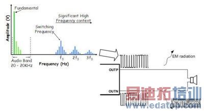
Figure 2: Frequency Content of Unfiltered Output Signal
The LC filter shown in Figure 3 is most commonly used, as it has a steep roll-off and is theoretically lossless. A second order Butterworth Low-Pass filter is recommended, due to its flat pass-band and desired phase response. For a single-ended output, the Butterworth filter can be designed using equations (5) and (6).
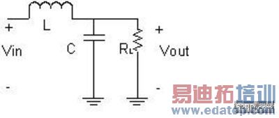
Figure 3: Single-Ended LC Low-Pass Filter
This figure assumes is the cut-off frequency in radians.
To convert the single-ended filter components calculations to component values for a bridge-tied load filter, the following conversions are required to form the filter shown in Figure 4:


Additional decoupling capacitors, Cg, are added to further suppress EMI emission. Cg is calculated to be one-tenth of the value of CBTL.
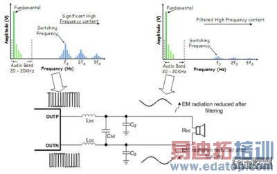
Figure 4: Bridge-tied Load LC Low-Pass Filter Implementation
Using the LC filter shown in Figure 4, the TPA3100D2 and TPA3101D2 EMI reference designs passed the FCC Part 15 Class B radiated emissions requirements with 21-inch speaker wires. Quasi-peak measurements were taken for four orientations, and the TPA3100D2 and TPA3101D2 EMI evaluation modules (EVMs) passed with at least 5.6-dB of margin. A plot of the peak measurement for the horizontal rear orientation is shown in Figure 5.
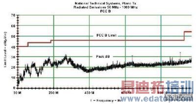
Figure 5: Radiated Emissions Pre-scan 30 MHz - 1000 MHz
Layout
When designing with class-D amplifiers, PCB layout is crucial for thermal, reliability, noise and distortion performance. EVMs (including Gerber files and BOMs) for the TPA3100D2 and TPA3101D2 are available at TI’s Web site, www.ti.com/audiodesigndoc, which can be used by engineers as a design example. Top and bottom copper masks are shown in Figure 6.
The ground plane needs to be large enough to dissipate the heat. The above-mentioned EVM is approximately 3.25 inches by 3.5 inches of double-sided one ounce copper on an FR-4 substrate and can achieve 20Wx2. Care should be taken to follow the footprint recommendations at the end of the datasheet. In particular, the density and size recommendations should be followed to ensure optimal heat dissipation.
In addition to providing thermal dissipation capabilities, it also is recommended to tie the analog and power grounds together at this thermal pad. This gives a star-connected grounding system, which has the lowest noise and best audio performance.
Tie the Cg capacitors on the output filter to the power ground; otherwise they may inject noise into the analog ground plane.
Any noise injected onto the ramp waveform or internal bias voltages will couple directly through to the outputs. This is why spread-spectrum operation suffers from an increase in noise floor; essentially the ramp signal is "noisy." It is important to pay attention to R6 (ROSC), C5 (VREG), and C10 (VBYP), as these are all sensitive analog components. In the EVM, they are tied together and returned to the star ground via terminal 17, which is the analog ground.
In addition, the power supply decoupling is of particular importance for class-D amplifiers. Note the two types of decoupling used: large electrolytics – C21 and C22, which provide current for low-frequency audio signals; and C18 and C19, which are high-frequency ceramic capacitors used to keep the voltage from drooping at the supply pins of the IC. It is critical that these two capacitors are located as close to the power supply terminals as feasible.
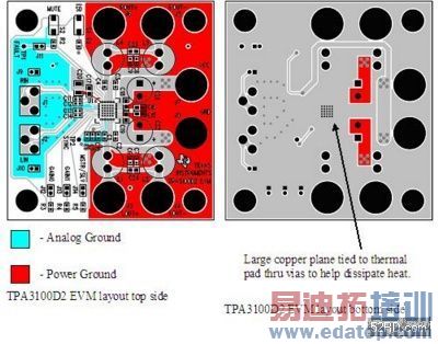
TPA3100D2 EVM layout available from TI’s Web site
Adaptive Dynamic Range Control
Virtually all analog input class-D amplifiers have a problem when driven into clipping. Once clipping occurs, the feedback architecture causes a characteristic dip when coming out of clipping. This is shown in Figure 7 as the "closest competitor" graph. This can cause undesirable audio artifacts. Prior to the TPA310x, the only solution to this problem was to prevent clipping by clamping the input signal.
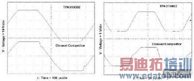
Figure 7: 1-kHz Sine Output at 10% THD+N and 8-kHz Sine Output at 10% THD+N
Figure 8 shows a block diagram of the basic channel of a class-D audio power amplifier. The signal at OTA forms the input to an integrating amplifier whose feedback is the output pulse width modulation (PWM) signals. The integrated input and feedback signals are converted to PWM using a triangle wave shaped ramp and a high speed comparator. This PWM signal is level-shifted to drive the bridge-tied load (BTL) output H-Bridge.
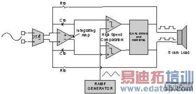
Figure 8: Block Diagram of TPA3100D2
At clipping, the outputs are at VCC and GND for an extended period of time. If the input forces the outputs further into clipping, the outputs of the integrating amplifier can move towards the positive and negative rails, beyond the ramp peaks and valleys. When the clipping condition is removed, it takes some time to discharge the integrating amplifier capacitors and return the outputs to a switching condition. This results in a notch in the audio wave form when the amplifier comes out of clipping and adds THD.
A patent-pending adaptive dynamic range control (ADRC) circuit has been added in the TPA3100D2 and TPA3101D2, improving the sound quality at higher power levels. This circuit has the goal of reducing excess distortion observed in class-D amplifiers, while driving maximum output levels.
The ADRC circuit works by monitoring the outputs of the integrating amplifier. When the outputs of the integrating amplifier exceed the ramp height, switches are closed around the integrating amplifier, reducing the gain of the channel. Figure 7 shows the improved response to a clipped sine wave. The clipping recovery circuit seeks to limit the maximum swing of the integrating amplifier by reducing the channel gain at full clipping. The ADRC circuit improves THD by 0.52 percent at 22W output power into 8 with a 20V power supply at 20 kHz input frequency.
Conclusion
Class-D amplifiers have been widely adopted in flat screen TVs due to the very real advantages they bring the designer. They allow cooler operation and elimination of heat sinks, which allows for tighter industrial design, an important product differentiator.
For designers switching from class-AB to class-D amplifiers, care must be taken to avoid common problems that may delay the design schedule. Following the suggestions in this article should minimize issues and speed the design process.

