- 易迪拓培训,专注于微波、射频、天线设计工程师的培养
视频系统:视频放大器/滤波器的模拟要求及实施(英)
Keep it all digital? Not yet.
In modern video systems it is common to utilize digital processing on both the front-end and back-end. This is due to the fact that the flexibility of these systems, coupled with their relatively low costs and integration of features, makes them very attractive to consumers. So why not simply keep video in the digital domain for all interconnections?
Digital video transmission has been around for years in the form of Serial Digital Video (SDV or SDI), but this was primarily limited to professional broadcast systems due to the costs involved. Newer digital transmission systems include DVI and HDMI. These systems are gaining ground in popularity, especially with high-end systems.
At the 2006 Consumer Electronics Show (CES), the "old" analog video transmission systems, namely component video, are still considered the primary interconnection method between set-top boxes and displays. Also, many "low-cost" video systems lacking high-end features are still widely used throughout the world. Where price is one of the most important buying factors for consumers, most people simply cannot afford HDTV’s. Therefore, traditional CVBS and S-Video will be around for many years to come.
Video nomenclature and background
Color information in video is derived from linear (tristimulus) Red, Green and Blue (RGB) components. Due to CRT display technology limitations, these fundamental colors need to be manipulated in a non-linear form known as gamma-corrected colors. To distinguish between true RGB and non-linear gamma corrected RGB, R’G’B’ will be used.
Traditional consumer video does not use R’G’B’ due to high bandwidth requirements on all three signals. To reduce bandwidth, costs, delay issues and modern day processing power, R’G’B’ signals are mathematically manipulated to create other forms of video signals.
The most important signal is brightness, or luminance. The International Commission on Illumination (CIE) stipulates the true definition of luminance (Y) shall be derived from linear RGB. Due to the non-linearity (Gamma) added to RGB, luminance no-longer holds true. Thus luma (Y’) is utilized and is technically the proper terminology for all consumer video systems.
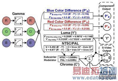
Similarly, chroma (C’), aka color information consisting of hue and saturation, is utilized rather than chrominance (C) due to the non-linear R’G’B’ terms being utilized. The color difference signals P’B, P’R, R’ – Y’, and B’ – Y’ are also referenced this way to denote the non-linear gamma corrected signals. Other terms including U, V, I and Q generally do not have the tick mark because these are mathematical equation elements and not used in the CIE color space. However, an argument could be made that these terms should have tick marks as they are based on elements that are non-linear. Table 1 shows a simplified RGB signal flow showing how these video terms are created, ignoring elements such as sync information.
View full size
Figure 1 – General RGB to consumer interface video signal flow
Analog video transmission – CVBS and S-Video
The original NTSC and PAL systems utilize a single wire transmission system, commonly called composite video baseband signals, or CVBS. Generally, these systems are limited in bandwidth to less than 6MHz. Note that the SMPTE (Society of Motion Picture and Television Engineers) 170M standard technically does not limit the Luma channel bandwidth in any way, only the Chroma or color difference signals. However, most systems will limit the signal to 4.2MHz due to RF transmission requirements.
The most significant voltage amplitude requirements of CVBS signals include a –40 IRE (–286mV for NTSC and –300mV for PAL) sync signal combined with a +100 IRE (714mV for NTSC and 700mV for PAL) video signal. These levels can vary slightly between standards, but the values shown represent the general voltages of these signals.
The 140 IRE peak-to-peak levels are true for a CVBS signal with 75 percent color saturation. However, many people forget that color can have 100 percent saturation. This leads to the CVBS signal having a possible voltage of 286mV + 935mV =1.221Vpp for NTSC and 300mV + 933.5mV = 1.2335Vpp for PAL. This is higher than any of the other standard video signals, and if forgotten, could lead to potential clipping of the video signal.
One of the biggest problems with CVBS signals is that Luma is combined with the Chroma signal. Because these signals can occupy the same frequency spectra, it is very difficult to separate the signals from each other without causing artifacts to appear. This is why there are many different video decoders with terms such as 2D, 3D, 3D adaptive, etc., comb filtering. Even with such extravagant techniques, artifacts can, and do, exist when trying to separate the two video signals.
The best way to eliminate this problem is not to combine the Luma and Chroma signals in the first place. S-Video does exactly this and produces an improved picture over CVBS. The bandwidth of S-Video, just like CVBS, is generally less than 6MHz. The only drawback to using S-Video is that two transmission wires must be used.
Analog video transmission – component video
To improve upon S-Video, component video was created to eliminate modulation of the Chroma signal that ultimately reduces errors. Component analog video maintains essentially the same Luma (Y’) information, but keeps the color difference information separated. P’B, not C’B which is used for the digital domain color difference, is the blue color difference signal. Likewise, P’R is the red color difference signal, while C’R is the digital domain red color difference.
The 1Vpp voltage amplitude requirement of component Luma is essentially the same as CVBS Luma. The sync is –300mV and the video information is 700mV on top of the sync level. The color difference signals, which the sync information is at the mid-point rather than the bottom-like Luma, allows for a 700mVpp signal.
Component analog video (Y’P’BP’R) includes several different formats. These formats include standard definition (SD), enhanced definition (ED) and high definition (HD) video. SD video includes NTSC based 480i (aka 525i) and PAL based 576i (aka 625i) where the ‘i’ term indicates interlaced video. These video systems have a video bandwidth up to 6.75MHz for Luma and up to 3.375MHz for P’B and P’R signals. The sync information is just like the CVBS signal except for the mid-point level for the color difference signals.
Enhanced definition (ED) video includes NTSC-based 480p (aka 525p) and PAL-based 576p (aka 625p). The ‘p’ indicates progressive scan and, thus, requires more bandwidth. The Luma signal is limited to 12MHz while the color difference signals are limited to 6MHz. The sync levels are just like the 480i requirements, but have a shorter (2.33us vs. 4.7us) width and refresh rate.
High definition (HD) video includes 720p, 1080i and 1080p. The Luma signal 720p and 1080i flavors have a bandwidth limited to 30MHz, while the color difference signals are limited to 15MHz. The Luma signal 1080p flavor is limited to 60MHz and the color difference signals to 30MHz. The SMPTE standards, 274M and 296M, allow for varying frame rates and sampling rates that can alter these analog bandwidths, but most systems utilize the above numbers. Note that the bandwidths and sync widths can, and do, vary for each respective profile as there are a considerable number of options (as much as 8 for 720p and 11 for 1080i/1080p) for each signal.
The voltage requirements for these HD video signals follow the same form as the 480i and 480p requirements. The Luma channel requires 1Vpp while the color difference channels require 700mVpp. The sync information is different in the respect that the HD signals utilize tri-level syncs. However, the bottom-level voltage excursions still follow the traditional 300mV single-sync pulse excursion that CVBS, 480i and 480p follow. Due to the tri-level sync and faster signal rates, the 720p sync width is as short as 0.54us, 1080i is as short as 0.59us, and 1080p can be as short as 0.296us.
Analog video transmission – computer and professional interfaces
Going into computer R’G’B’ video signals opens up a very large matrix of signal requirements based on pixel resolutions and refresh rates based in large part on Video Electronics Standards Association (VESA) standards. Note that in the computer world, RGB is commonly used, although in reality these are also non-linear gamma corrected signals and should realistically be R’G’B’. The biggest difference between the consumer video signals and R’G’B’ is that all three R’G’B’ signals require the exact same signal bandwidth.
R’G’B’ signals have the highest frequency requirements that can reach beyond 148.5MHz (1920 X 1440 @ 75Hz) and undoubtedly will be going even higher. Thus, processing power is substantially increased to handle three signals with very wide bandwidths. Systems such as Y’P’BP’R have much less processing power requirements (due to 4:2:2 processing) resulting in a cheaper system. Timing of all three signals is critical or else color shifting can occur. To produce pure white, all three signals must be 100 percent while only one signal, Luma, is required for the consumer signal. Generally, this allows for easier calibrations as brightness or Luma is separated from the hue/saturation, chroma or color difference, information. Timing is also not as critical with the consumer video signals like R’G’B’.
Voltage requirements for computer R’G’B’ is just like the Luma signal requirements of 700mVpp. The only difference is that the sync information may or may not be included with the signals. Sync information can be completely separate and in this case requires two separate signals – Horizontal and Vertical Sync lines. Sometimes these are also combined into one signal – H + V Sync. Many times the sync information is included on the Green signal – R’G’sB’. Other times the sync information is included on all three signals – R’sG’sB’s or sR’G’B’. When sync is embedded with the video signal, the amplitude is 300mVpp, just like the traditional Luma signal. Obviously the sync duration depends on the resolution and refresh rate of the signal. This can vary from 3.8us (640 X 480 @ 60 Hz) to as short as 0.74us (1920 X 1200 @ 85Hz) or further such as the reduced blanking 1920 X 1200 @ 60Hz requirement of 0.208us.
Lastly, in professional and broadcast systems, G’B’R’ is utilized. The SMPTE component standard stipulates that the Luma information is placed on the first channel, blue color difference is placed on the second, and red color difference is placed on the third, which is consistent with the Y’P’BP’R nomenclature. Because the luma channel (Y’) carries the sync information and the green channel (G’) also carries the sync information, it makes sense that G’ be first. Since the blue color difference channel (P’B) is next and the red color difference channel (P’R) is last, it also makes sense to place the B’ signal on the second channel, and the R’ signal on the third channel. Thus, hardware compatibility is better achieved by using G’B’R’ rather than R’G’B’.
Video and sync amplitudes for each G’B’R’ signal are the same as the respective Y’ requirement for each of the following standards respectively – 480i/525i, 576i/625i, 480p/525p, 576p/625p, 720p, 1080i and 1080p. Note that for many G’B’R’ systems sync is embedded on all three channels, but may not always be the case in all systems. The bandwidths required for these systems are essentially the same as the Luma bandwidth requirements previously mentioned for each respective SD, ED, and HD standard. Just like the computer R’G’B’ signals, timing of each signal is critical to the video signal along with the calibration of the display.
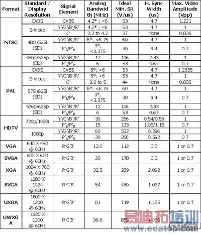
Table 1 lists some of the analog requirements for video signals. Because there are many other variations for each video system, these numbers represent a good starting point. For ideal minimum slew rate numbers, the general formula SR = (2 Pi F 0.707 Vpeak * 2) was used with Vpeak being 1V (2Vpp) assuming an output buffer under worst case conditions, 0.707 used as the –3dB amplitude at a given -3dB frequency point, and a factor of 2 multiplier buffer just to be safe. In a real system, the video signal does not need to go from 0V to 1V (1Vpp or 0.5Vpeak), but more like 0V to 700mV (350mVpeak) to go from black to white. For an input buffer, the amplitude is one-half the output buffer requirements. So, use information in Table 1 only as a starting point.
View full size
*Generally used limit, but not required.
Table 1: Fundamental analog video signal requirements
Analog filtering
Why is filtering even used in analog video? As stated initially, it is common to convert the analog video signal into the digital domain, or visa-versa. For displays and receiver boxes such as DVD-Recorders, this implies the use of analog-to-digital converters (ADC). For set-top-boxes and DVD players, this implies the use of digital-to-analog converters (DAC). Both ADCs and DACs have images dictated by the sampling frequency. These images can "fold" down into the baseband and cause picture quality problems.
Even if a DAC or ADC has digital filtering, analog filtering external to the converter is still needed. Images will continue to exist in these systems unless filtering is done. The reason is simple: the converters are still sampling and as such, will have images.
To meet SMPTE filtering requirements, the entire system should strive to meet the standard, not the filter by itself. Many DACs already have digital filtering and interpolation filters. This by itself helps considerably. Coupled with a respectable analog filter and the SMPTE requirements can be approached.
To maintain good picture quality, these data converter images must be filtered out (see Figure 2). This is where placing an analog filter into the signal path becomes very important. Using a filter to eliminate DAC images (aka, reconstruction filter) is important in a system that utilizes a DAC. However, is a filter required for an input device such as a display? Absolutely!
Because a display can connect to virtually any source, there is a possibility that the source may not have filtering, or very poor filtering. Additionally, if there is any EMI interference, the ADC anti-aliasing filter will minimize any visual problems. As a side benefit, an anti-aliasing filter will also reduce the general noise floor of the signal by reducing bandwidth.
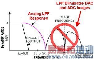
Figure 2 – Standard definition video DAC images reduced by filtering
Eliminating both DAC and ADC images will improve visual quality. However, what filter type and how many poles should be used? What corner frequency, flatness, and group delay is best for the video signal? If ten engineers are asked this question, there probably will be ten different answers.
As stated previously, the corner frequency for each video signal can be determined relatively easily. It is desirable to have the flattest pass-band as possible with the most attenuation near the data converter sampling frequency. Using only this requirement an elliptic or Chebyshev type of filter comes to mind. If the only concern is amplitude flatness and attenuation, then these filters would be ideal – allowing any system to meet SMPTE filter characteristics. But, group delay must NOT be forgotten because the SMPTE standard also includes group delay limits and a system should strive to meet BOTH of these elements, not just one.
Group delay is defined by the change in phase (radians/second) divided by the change in frequency. The flatter the group delay, the more linear the phase change is over frequency. In the time domain, this is very important for pulse responses. The analog video transmission system can be primarily considered a time-base system. Imagine a video display changing from black, to white, and back to black for every pixel. This means the video signal voltage will go from 0mV to 700mV as fast as possible for one pixel, and then back to 0mV for the next pixel. If the group delay variation across the frequency band changes considerably, overshooting and ringing will occur. Elliptic and Chebyshev filters will have this ringing response due to an excessive variation in group delay. On a display this can appear as ghosting or fuzzy edges – which is not good, even though the attenuation is very good.
As such, a good balance must be made between amplitude flatness, corner frequency, attenuation and group delay variation to achieve an acceptable video filter – which is why there are so many different views on this subject. The general consensus is the Butterworth filter is a respectable compromise for consumer video. It has a maximally flat amplitude response, a reasonable rate of attenuation and respectable group delay. The Butterworth filter is not ideal, but usually is good enough for the system.
Examples of filters
The new THS73x3 series of integrated filter/amplifiers from Texas Instruments utilizes a modified fifth-order Butterworth filter. It has been modified by slightly reducing the Q, or peaking factor, in an effort to minimize group delay variations. The drawback is the flatness is not as ideal as a true Butterworth, but the attenuation is nearly identical.
Five poles were chosen rather than four or six poles because odd-order filters have a true real-pole rather than all complex-poles that even-order filters realize. While the real-pole may be considered irrelevant by some people, real world experience has proven that a real-pole can be beneficial in active filter systems, especially when implemented by the Sallen-Key architecture. The Sallen-Key system has a high-frequency path through the system and passes high frequencies relatively easy above the amplifiers bandwidth limitation. A real-pole in the system shunts any high frequency signals to ground above and beyond the amplifier’s bandwidth limitation. Thus, it helps make sure the filter remains a filter at very high frequencies.
In an effort to show the effects of group delay and amplitude flatness, another filter was simulated using the Filter Pro Program, available from TI’s web site. A five pole, 0.5dB Chebyshev filter with a corner frequency (–0.5dB down) of 10MHz was simulated. Additionally a fifth-order modified Butterworth filter with a corner frequency (–3dB down) of 8.5MHz was also simulated. Figure 3 shows the amplitude responses of each filter. The Chebyshev filter has the 0.5-ripple expected, but the "flatness" is out to 10MHz, greatly exceeding the Buttwerworth’s flatness. Additionally, the attenuation rate is much higher with the Chebyshev achieving over 56dB of attenuation at the critical 27MHz point. The Butterworth "only" achieves 46dB of attenuation at 27MHz. In reality, this is generally plenty enough for a video system.
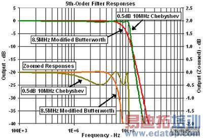
Figure 3 – Filters amplitude responses
Figure 4 shows the phase and group delay responses of the filters. The Chebyshev filter has considerably more variations in the group delay compared to the Butterworth filter, especially at the corner frequency. This can also be seen in the phase responses. Keep in mind that for most systems, the absolute value of the group delay is essentially irrelevant. It is the variations in group delay that are more important.

Figure 4 – Filters group delay and phase responses
Figure 5shows the impact of a pulse response on each filter system. The pulse has a transition time of 37ns, which is in theory what a 27MHz DAC step could provide. The modified Butterworth filter, with a much smaller group delay variation, has a much improved response. The overshoot is almost the same, but the Chebyshev filter continues to have a ringing response for a considerable amount of time.
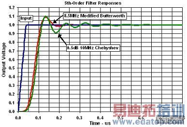
Figure 5 – Filters Pulse Responses
Figure 6 shows a close up view of the same pulse response. Many video systems try to keep variations less than 1 IRE, or about 7mV. The minor lines shown in the figure are 10mV. As such, the Chebyshev response will have at least 1 IRE variation up to about 480ns after the pulse was applied, as compared to the modified Butterworth "settling" at about 220ns. This can cause a negative effect such as ghosting or fuzziness.
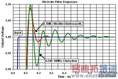
Figure 6 – Close up view of filters pulse responses
When using active filters, keep in mind the higher the Q of the filter, the higher the amplifier bandwidth needs to be. Using Bessel or Butterworth filters, or even high order versions, keep the Q of each stage relatively low. A filter designed with Elliptic or Chebyshev responses have much higher Q values and can demand a much higher bandwidth amplifier to implement reasonably. Otherwise, the impact of the amplifier on the filter will alter the desired responses. Granted these can be designed out by modifying component values, but amplifier-to-amplifier variations start coming into play much more significantly than before.
Passive vs. Active Filters
Passive filters are commonly found in systems today because they can be fairly inexpensive. However, drawbacks include PCB area, extra component inventory, more assembly time, pass-band signal loss, electro-magnetic influences on inductors and tolerances. Inductors and capacitors with +/-10 percent variations are common, especially for low-cost components. However, these tolerances can have a major impact on the filter response due to individual component-to-component variations and the fact that several poles are involved.
Monte-Carlo analysis is a useful tool to see the impact on performance for passive filters. Simulations show that there will be considerable variations in corner frequency, flatness, attenuation and peaking when using +/- 10 percent tolerance components.
Using active filters can improve the shortcomings of passive filters. In a semiconductor process such as BiCom-3 used in the THS73x3 devices, element-to-element matching is typically very tight. It is not uncommon to see less than one percent variation from resistor-to-resistor and capacitor-to-capacitor. Keep in mind that there will be significant variations in absolute component values. It is not uncommon to see 10 percent or more, depending on the component and the type of component. This will impact the corner frequency and attenuation characteristics of the filter.
However, in an integrated active filter design such as the unity gain Sallen-Key filter utilized in the THS73x3, the variations in flatness and peaking can be very tightly controlled. Sensitivity analysis of a unity gain Sallen-Key filter (not be replicated here due to space constraints) shows that as long as resistor-to-resistor and capacitor-to-capacitor matching is very tight along with unity gain, essentially the only variations will be with corner frequency with no variations in Q. A variation in Q leads to significant group delay variations which is undesirable. As long as high-quality capacitors and resistors are used, and assuming the amplifiers natural bandwidth is much higher than the corner frequency of the filter, the active filter can have much better controlled characteristics than a passive filter. Additionally, an active filter typically uses much less PCB area and with only one component to procure, inventory is reduced significantly.
Another important aspect about multi-pole passive filters is that their corner frequency cannot be changed easily without becoming extravagant and costly. An active filter designed with selectable filters is very easy to implement. This may not be the most attractive feature in a CVBS and S-Video system as the filter frequency does not need to be changed. However, for a component video system or G’B’R’ system, changing the filter frequency can be very beneficial due to the fact that it can be SD, ED, or HD (720p/1080i) or 1080p HD.
This is especially important for receiver systems that accept components Y’P’BP’R or G’B’R’. For example, a fixed 35MHz passive filter was used to allow all component signals into a display. However, what happens if a 480i or 576i SD component signal was applied to the input? A common DAC sampling frequency is 27MHz for these type of signals. If the DAC has no reconstruction filters, the images appearing on both sides of the 27MHz fundamental will come directly through the display’s passive 35MHz filter. The result is no attenuation of the images, and the display will most likely appear very poor.
This is also a possibility for the ED 480p/576p signal. These types of signals generally have a sampling frequency of 54MHz and the video bandwidth is 12MHz. As such, the second Nyquist zone image will start to appear at 42MHz. If the passive filter is at 35MHz or higher, there will be very little attenuation of this image, which again can lead to poor image quality.
This is where a selectable filter becomes very important, for both the DAC side utilizing the THS7303 and the ADC side utilizing the THS7353. These integrated filters/amplifiers incorporate a selectable fifth-order modified Butterworth filter which can be set for 9MHz for SD signals, 16MHz for ED signals, 35MHz for HD 720p/1080i signals, or >150MHz bypass mode for very fast signals such as 1080p. Figure 7 illustrates this point.
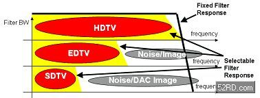
Figure 7: Fixed filter vs selectable filter benefits with Y’P’BP’R signals
For added flexibility, each channel of the THS73x3 is individually controlled. With this feature, someone can select 35MHz for the Luma channel, and 16MHz for the color-difference channels, which is acceptable based on the analog signal bandwidth requirements. One drawback is that the delay associated with the different filters will vary by the same frequency scaling. This could result in timing issues if not dealt with through digital processing.
High-end systems also benefit where phase shift and group delay are very important parameters. Here a 16MHz filter could be used for SD signals, ensuring a very smooth and flat response throughout the SD spectrum with essentially no overshoot in the time domain pulse response. This is also applicable with 35MHz filters for ED signals or bypass mode for HD signals.
Lastly, passive filtering will have significant variations in impedance over frequency. The can cause interaction issues with both DACs and ADCs. Additionally, this could lead to ringing issues if the source resistance or terminating resistance is outside of the 75ohm requirement. The THS73x3 active filter/amplifiers mitigate this problem. Their input impedance can be greater than 1Mohm, while their output impedance is less than 1ohm at 10MHz. This can eliminate issues with ADC kick-back issues or decoder input clamping issues.
Power supply voltages and power dissipation
Most video systems use single-supply data converters with a 3.3V supply. If this supply could be used for the video filter/amplifier, it would make the system easier to use and potentially could eliminate a power supply or two – resulting in lower costs. The THS73x3 parts exploit this capability by operating from 2.7V to 5V single-supply. The BiCom-3 process was designed to operate at these voltages and has no performance disadvantage over the entire operating range. In fact, some specifications such as differential gain and phase improve with lower power supply voltages.
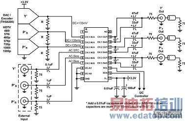
Figure 8 shows a typical configuration for the THS7303 amplifier buffering a DAC and accepting an external input, while utilizing a 3.3V power supply with SAG correction on the output. This figure should be a reference for the remainder of this paper.
View full size
Figure 8: Typical system configuration for the THS7303 in a 3.3V single-supply, DAC DC+Shift and AC-STC and AC-bias coupled inputs, along with SAG corrected output line driving.
Another factor to consider is power consumption. It is not uncommon to find 5V single supply parts similar to the THS73x3 products. But many consume over 500mW of power with some as high as 1.2W. This can result in very high die temperatures and can easily impact long-term reliability. The THS73x3 consumes only 55mW of power while running on 3.3V supply. This virtually eliminates thermal and reliability concerns.
To conserve power, each channel can be shutdown individually. If all channels are shutdown, the current consumption is less than 1uA. Together, these parts are applicable for power sensitive systems such as portable or USB powered systems.
Signal coupling
One concern about running from a single-supply down to 2.7V is whether or not the video signal will have clipping. This is where proper DC-biasing is very important in the design. With so many different types of video systems and designs, having the flexibility to properly bias the THS73x3 is critical.
If the THS7303 or THS7313 6dB gain amplifier is designed into a system which is driven from a ground-referenced DAC or encoder, the DC input mode is ideal. The question is how low is the voltage created by the DAC? If the sync signal (which is typically the lowest voltage of a video signal) is below 50mV, then the output of the 6dB amplifier needs to generate voltage less than 100mV. This can be very difficult for any amplifier due to transistor saturation limitations, which exists in both CMOS and bipolar amplifiers.
To remove this limitation, all THS73x3 products have a DC + Shift mode that adds an internal DC voltage offset to the video input signal. This offset is internal only and will not impact the applied signal. This offset will ensure that even if 0V is applied to the input of the THS73x3, the output will not saturate and clip.
If the DAC output voltage only goes down to 100mV, then the DC input mode is best. This mode does not add an offset into the system as it is not required. Keep in mind that there are offsets in any amplifier and this is true for the THS73x3. This offset voltage is typically small, but does have part-to-part variations.
If the DAC is referenced from a power supply such as 3.3V or 1.8V, or is an external input, then utilizing AC coupling is the best mode. AC coupling allows the THS73x3 to ignore the source DC-bias point and will re-establish its own DC-bias point. The AC coupling options include AC-bias or AC-sync tip clamp.
AC-biasing is very simple. The THS73x3 has two resistors that create a voltage divider between the power supply and ground. The input impedance of this mode is about 20kohm. As such, the capacitor used should be large enough to ensure any tilt or droop issues are minimized. In general, a 4.7uF to 10uF capacitor will minimize any tilt problems. This mode is best used with Chroma or color difference signals. It can also be utilized for the Luma signal, G’B’R’ signals, or computer R’G’B’ signals. Since the signal is AC-coupled and the DC-bias point varies with the average signal level, it is best to utilize the AC-Bias mode with signals that have sync information with 5V supply to ensure no clipping will exist.
The patent-pending AC-sync tip clamp (STC) mode (Figure 9) is best for signals with syncs at the lowest point of the video signal. This implies the Luma (Y’), G’B’R’ with sync, or computer R’G’B’ with sync signals are best utilized with AC-STC mode. The sync-tip clamp system in the THS73x3 has an internal current-sink to discharge the coupling capacitor, a filter to minimize interaction with high-frequency interference signals that may be present, an amplifier that monitors the difference between the voltage on the input and the reference voltage, and finally a transistor to charge the capacitor when the signal goes below the reference. As such, this is a dynamic system that does not rely upon timing in any way. This type of system is also generally called a DC-restore system rather than a diode clamp system. The problem with diode clamp systems is they react to any high-frequency signal or overshoot. This can result in an undesirable excessive DC-bias point shift and can clip the signal.
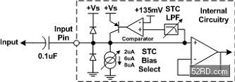
Figure 9: AC-STC basic system
The flexibility of the THS73x3 family allows the user to tweak some of the AC-STC functions. This includes the STC filter between 500kHz, 2.5MHz and 5MHz. This is important as the horizontal sync width varies with the signal standard applied (see Table 1). If the 500kHz filter was utilized with a 720p Luma signal, the STC circuit would never engage and the system would float. But, if a CVBS signal is noisy or has considerable ringing, the 500kHz filter would be best to minimize any DC-bias shift internal to the THS73x3.
The AC-STC allows a discharge current to be selected. If the voltage appearing at the input to the THS73x3 drops below the reference voltage, the system can charge as much as 2mA of current to increase the voltage. What happens if the voltage is considerably higher than the reference voltage? The discharge current will reduce the voltage on the capacitor at a rate equal to I/C = dV/dT. This current is selectable from about 2uA, 6uA, and 8uA. Having a high discharge current allows the system to capture a signal quickly or increase hum rejection (when 50 or 60Hz line signals couple into the system). Other systems require a very low discharge rate to improve line-tilt or droop. This is when a video signal is held constant over the entire line. Because of the AC-coupling and discharge current, the DC signal will tilt downwards. It is generally acceptable to have less than 1IRE of tilt over a line. This selectability allows the system to connect to essentially any outside source without requiring the need to change input capacitors manually.
Figure 8 also showed the 2:1 input MUX feature. This, coupled with the user configurable input coupling that is completely independent of the other channels, allows the THS73x3 to be utilized in many different systems.
Output capabilities
The most common output configuration of a line driver amplifier is to use AC-coupling. This is done to eliminate any possible DC-bias current flow and makes the system more universal. It is common to use between 220uF and 1000uF capacitors on the output of the amplifier to reduce line tilt.
In some systems, the DC-bias current is not a major concern. Instead, cost and PCB size may be more important. The THS73x3 allows DC-coupling without problems due to the rail-to-rail output amplifier stage. The output swing reaches within 100mV of the power supply and ground and can drive up to 80mA of current.
Other systems may require AC-coupling, but PCB size is also important. The flexibility of the THS7303 and THS7313 allows a method to achieve this goal – SAG correction. SAG correction requires two capacitors, but these capacitors are much smaller – nominally 47uF and 33uF and can achieve about the same tilt performance as a 330uF capacitor. Increasing these values to 68uF and 47uF respectively results in performance similar to a 470uF capacitor.
The SAG function obtains this result by utilizing an increase in gain as the frequency decreases. The amplifier gain counter-acts the 47uF capacitor drop resulting in an extension of the realizable pass-band. The 33uF capacitor is chosen to obtain a small peak, or Q-enhancement. This "cheats" the video system into achieving a respectable line-tilt or droop, especially with a field square wave signal.
Figure 10 shows the basic configuration of how SAG is implemented in the THS7303 and THS7313. SAG correction is also used by other manufacturers, but those systems often require much larger capacitors or larger power supplies to account for the larger DC gain that occurs in the system.
It is relatively easy to see how SAG functions. At DC, the gain increases due to the internal 675ohm resistor added in series with the 878ohm feedback resistor. At high frequencies where the output capacitor and SAG feedback capacitor are shorted out, the 675ohm resistor is in parallel with the 150ohm resistor, resulting in a 6dB system gain. This DC gain enhancement along with the proper ratio of capacitors allows the SAG function to simulate a much larger capacitor.

View full size
Figure 10: System level diagram of THS7303 showing the SAG feature
Figure 11 shows the results of a 47uF + 33uF SAG connected output along with a 47uF, 100uF, and a 330uF traditional output configuration as shown at the Video Out point in Figure 10. This shows a small amount of peaking occurring that extends the performance of the system even further than if there were no peaking. Figure 12 shows the output voltage of the amplifier and the SAG feedback voltage.
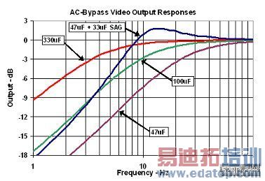
Figure 11: Video output at receiver responses
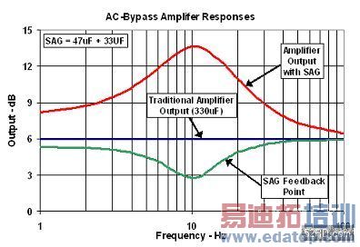
Figure 12: SAG voltage responses and traditional response
The THS7353 output is configured differently than the THS7303 and THS7313. The nominal gain of the THS7353 is 0dB, or unity gain. This is because the THS7353 was explicitly designed for an input system, such as for displays or DVD-Recorders. The front-end of these inputs are typically video decoders or video ADCs / scalers. As such, the allowable input range of these converters is typically less than 1.3Vpp. Hence the unity gain requirement. Additionally, the loading of an ADC is vastly different than a 150ohm line. ADC front-ends are typically very high impedance, greater than 10kohm, and typically have about 5 to 10pF of capacitance. As such, the THS7353 was optimized for this loading which is a very different compensation than required for driving video lines.
Also, the THS7353 can have gain adjustments configured externally. This allows the user to configure the gain to their needs. Sometimes it is a simple 0.5dB to 1dB flat gain. Other times it is desirable to counteract a SinX/X characteristic that may exist with a DAC. In other systems a long cable may be connected which has skin-effect losses that need to be compensated as shown in Figure 13.

View full size
Figure 13: THS7353 driving an ADC with cable equalization
In some systems, the DAC output voltage capability requires higher gains than the 6dB gain offered by the THS7303 or THS7313. There are two simple ways to solve the problem; use the THS7353 and an external gain resistor, or use the THS7303 / THS7313 SAG feedback point. If an external resistor is placed between the SAG feedback point and ground, the gain of the amplifier becomes:

Figure 14 shows this configuration.
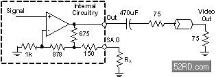
Figure 14: THS7303/THS7313 with higher gain configuration
For example, adding an external 726ohm resistor between SAG and ground results in a system gain of 4V/V, or 12dB. The drawback to this feature is the DC output level also increases and care must be taken to ensure there are no clipping issues. Additionally, the output amplifier is a voltage feedback amplifier (VFB) which has a gain-bandwidth (GBW) product limitation. While this will not seriously affect the filter characteristics, it will affect the THS7303 filter bypass bandwidth inversely with gain. For example, with a gain of 4V/V, the bandwidth of the THS7303 in bypass mode becomes approximately 90MHz. The THS7353 also has a GBW limitation with a default unity gain. Increasing the gain beyond 2 or 3V/V will seriously start reducing bandwidth. Additionally, the compensation of the THS7303 was designed explicitly for driving the video line and as such, is best suited for DAC buffering.
Control and interface
To allow these features and flexibility to exist in the THS73x3 products, I2C control is employed. GPIO was considered, but there would need to be at least 8 to 10 pins to control all the options on a reasonable manner. SPI was also considered due to its higher immunity to noise and timing over I2C. But, because almost every encoder, decoder, video processor, etc., already uses I2C, it makes perfect sense to use the same system already there. To ensure there are no I2C address conflicts, there are 2 pins that allow up to 4 addresses to be set on the THS73x3.
Conclusions
The flexibility of the filters, input biasing, input MUX, output configuration, I2C control, single supply with operation from 2.7V to 5V, and very low power consumption is unmatched in the industry. Couple all of these features with a very reasonable price and the THS73x3 represents a major breakthrough in video filter amplifiers that should work in just about every video system.
上一篇:D类音效放大器的2W1H:What、Why & How(上)
下一篇:平板音频设计以平面屏幕展现跌宕起伏的音频(英)

