- 易迪拓培训,专注于微波、射频、天线设计工程师的培养
根据高效数据采集系统选择与设计最佳过滤器(英)
One of the jobs of a circuit designer is to build a measurement system that provides valid input-to-output data as defined by the system requirements over a given frequency range. The four possible elements of a signal path include a gain/signal conditioning cell, an anti-aliasing filter, an analog-to-digital converter (ADC) and a digital processing block. Figure 1 shows this type of system with a simplified analog signal conditioning path. The gain/signal conditioning cell executes functions such as analog conversions from current to voltage, amplitude gain, and/or voltage level shifts.
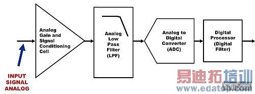
Figure 1: The classical analog signal path from sensor to digital processor is comprised of four cells. These four cells can be independent of each other or combined, but these fundamental functions in the signal path in this diagram will still occur.
Following this cell is an analog-filter stage, which reduces out-of-band frequencies that can degrade the analog-to-digital (A/D) conversion. The A/D conversion is next in line in this signal conditioning path. Conversion from the ADC transmits a digital representation of the gained, filtered analog signal to a digital processor.
The validity of the output signal of each stage is determined in terms of amplitude integrity, linearity and frequency content as it relates to the input signal. Of the three analog functions shown in Figure 1, signal contamination is most apt to occur as the signal passes through the ADC. Although one of the primary intents of using a filter in the position prior to the ADC is to remove frequencies above half of the ADC sampling frequency, the filter can also introduce anomalies such as ringing, propagation delay and in-band amplitude distortion.
This article describes when to use an analog filter and when the digital filter more appropriate. Additionally, the article shows how to select the correct anti-aliasing filter for three different types of sensor signals; a dc (static) temperature signal, a multiplexed step response, and an ac (dynamic) photosensing signal.
The case for using a digital filter
The system shown in Figure 1 includes an analog filter before the ADC and a digital filter afterwards. It is obvious why these two filters are at these particular points in the circuit. However, the ramifications of these positions may not be obvious. There are a number of system differences when the filtering function is in the analog domain, rather than the digital domain. Every analog signal has both high- and low-frequency content, as well as a magnitude associated with the signal and noise.
The ADC reliably converts input-signal magnitude and frequency as long as the signal frequency is below the converter’s input-stage bandwidth. At frequencies above half of the ADC’s sampling frequency the magnitude is preserved, but the same is not true for the signal’s frequency value. The A/D conversion process alters signal frequencies above half of the ADC sampling frequency. This alteration or aliasing makes it impossible to discern the difference from signals at less than half of the sampling rate and signals that are greater than half of the sampling rate. The plots in Figure 2 illustrate this concept.
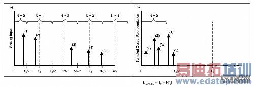
Figure 2: A system that has a sampling frequency at fs (a) will digitize signals with frequencies below fs/2 as well as above. Input signals below fs/2 will be reliably digitized while signals above fs/2 will be folded back (b) and appear as lower frequencies in the digital output.
In both parts of Figure 2, the x-axis identifies the frequency of the sampling system, fS. Figure 2a shows five segments of the frequency band. Segment N = 0 spans from dc to one-half of the sampling frequency. In this bandwidth, the sampling system will reliably record the frequency content and the magnitude of an analog input signal. In the segments where N ý¾ 0 the frequency content of the analog signal will be recorded by the ADC in the bandwidth of the segment N = 0 on the left side of this figure. Mathematically, the higher frequencies (2, 3, 4 and 5) will fold back with the following equation:
fALIASED = ¦fIN − NfS¦
Figure 2b illustrates this fold-back phenomenon as the signal is converted, where signals 2, 3, 4, and 5 appear at lower frequencies than in Figure 2a.
For example, suppose the sampling frequency (fS) in Figure 2a of the system is equal to 100 kHz and the input frequency is:
fIN(1) = 41 kHz
fIN(2) = 82 kHz
fIN(3) = 219 kHz
fIN(4) = 294 kHz
fIN(5) = 347 kHz
The sampled output in Figure 2b will contain accurate amplitude information for all of these input signals. However, four of the signals will fold-back into the frequency range of dc to fS/2 or dc to 50 kHz at the output of the converter. The frequencies of the input signals will change to:
fOUT(1) = ¦41 kHz − 0 x 100 kHz¦ = 41 kHz
fOUT(2) = ¦82 kHz − 1 x 100 kHz¦ = 18 kHz
fOUT(3) = ¦219 kHz − 2 x 100 kHz¦ = 19 kHz
fOUT(4) = ¦294 kHz − 3 x 100 kHz¦ = 6 kHz
fOUT(5) = ¦347 kHz − 4 x 100 kHz¦ = 53 kHz
Note that all of the signal frequencies above fS/2 have a change in frequency at the output of the converter. It will be impossible to remove these signals after an A/D conversion.
A low-pass analog filter removes superimposed higher frequency noise from the analog signal before it reaches the ADC. This also includes extraneous noise peaks. The digital filter is programmable and, depending on the digital filter design, the designer has the capability of programming the cut-off frequency and output data rates on the fly. Implementing a high-pass filter and a second, low-pass filter can be a digital or analog filter function. The variety of digital filters includes analog-style filters such as Butterworth, Bessel, Chebychev or elliptic, as well as the classical digital filters such as the finite impulse response (FIR) filter or a Fast Fourier Transform (FFT).
There are times to build a filter with analog hardware and times where it is appropriate to implement it with a controller or processor in firmware. An analog low-pass filter should be in every circuit where there is an A/D conversion in order to reduce higher frequency noise. This is true whether the ADC is a Successive Approximation Register (SAR), sigma-delta, pipeline, or dual-slope. The placement of low-pass filter in the circuit must always be on the analog side in front of the converter as shown in Figure 1.
Low-pass filter basics: frequency response
Excluding the hardware implementation, the description of a low-pass filter uses the combination of frequency domain and time domain tools. Two standard plots, the magnitude and phase response, describes the filter in frequency domain. This information portrayed with these two plots facilitates decisions concerning noise reduction and aliasing issues. The time domain plot offers a different perspective of the same information found in the two frequency domain plots of Figure 3. The time domain plot, Figure 4, provides information concerning settling time, overshoot and propagation delay of the filter’s response.
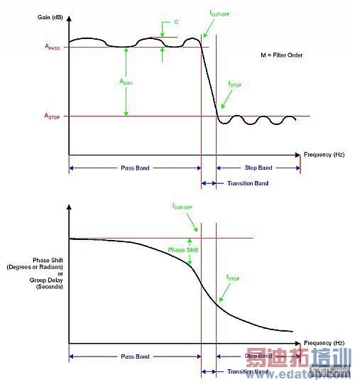
Figure 3: In the frequency domain, there are five parameters, fCUT-OFF , fSTOP , AMAX, Phase Shift and M for the low-pass filter.
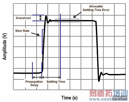
Figure 4: This diagram shows the output of a filter that is responding to an input pulse or step signal. In the time domain, a low-pass analog filter can be specified with five parameters, propagation delay (tD), slew rate (SR), overshoot, its allowable settling time error (ý) and settling time (tS).
In the gain-versus-frequency plot in Figure 3, the cut-off frequency (fCUT-OFF) for Butterworth and Bessel filters of a low-pass filter is at the frequency where the response is 3 dB below the gain of the filter at dc. For a Chebyshev filter, the cut-off frequency is the final point where the response leaves the ripple band ε.
The phase versus frequency plot for a filter indicates the phase relationship between the input and output signal. Units of measure in the phase plot can be degrees or radians. The information from the phase plot in Figure 3 is somewhat instructive, but a more useful way of looking at the phase information is to examine the filter’s group delay. The group delay, in seconds, of a filter is equivalent to the (change in phase/change iný’frequency) at each frequency.
It is easy to translate the group delay of a filter into the time domain. If the group delay is linear and tracks the magnitude plot, the filter step response will be well behaved with very little ringing. If the group delay does not track the magnitude plot, the filter response to input steps will have an overshoot and ringing.
The frequency span from dc to the cut-off frequency is the pass band region. The magnitude of the response in the pass band is defined as APASS as shown in Figure 3. The response in the pass band can be flat with no ripple as is with the Butterworth or Bessel filters. Conversely, a Chebyshev filter has a ripple up to the cut-off frequency. Epsilon (ε) is the magnitude of the ripple error of the Chebyshev filter.
By definition, a low-pass filter passes lower frequencies up to the cut-off frequency and attenuates the higher frequencies that are above the cut-off frequency. An important parameter is the filter system gain, AMAX. This is defined as the difference between the gain in the pass band region of the filter and the gain in the stop band region or AMAX = APASS - ASTOP. In the case where a filter has ripple in the pass band, the gain of the pass band (APASS) is at the bottom of the ripple.
The frequency at which the desired minimum attenuation occurs identifies the stop-band frequency, fSTOP, for filters that do not have a bottom ripple response. Although it is possible that the stop-band has a ripple, the minimum gain (ASTOP) of this ripple occurs at the highest peak of the response. The system specifications determine the minimum attenuation level.
As the response of the filter goes beyond the cut-off frequency, it falls through the transition band to the stop band region. The filter approximation type and the number of poles determine the bandwidth of the transition band. Examples of filter approximation types are the Butterworth, Bessel, or Chebyshev, to name a few. The number of poles in the transfer function of the filter determines the order (M) of that filter. For instance, if a low-pass filter has three poles in its transfer function, it is a third order filter.
Generally, as the implementation of the filter design uses more poles, the transition band will become smaller. Ideally, an infinite order, low-pass (anti-aliasing) filter performs with a "brick wall" style of frequency response, where the transition band is as small as possible. Practically speaking, this may not be the best approach for an anti-aliasing filter solution. With active filter design, every two poles require an operational amplifier. For instance, the implementation of a 32nd order filter requires 16 operational amplifiers, 32 capacitors and from 32 to 64 resistors (depending on hardware circuit configuration). This order of filter is also difficult to implement as a stable solution. Additionally, each amplifier would contribute offset and noise errors into the pass band region of the response.
Low-pass filter basics: step response
The plots in Figure 3 describe low-pass filter performance in the frequency. The plot in Figure 4 describes the same low-pass filter performance in the time domain.
In Figure 4, the propagation delay (tD) represents the amount of time that it takes for the filter to respond to the input signal. The propagation delay time is the inverse of the phase (Figure 3) of the fundamental of the input signal. After this delay, the filter goes into a slew condition and the output of the filter attempts to catch up to the input signal.
The units for the slew rate (SR) are volts per second. As the output signal approaches the input signal level, the filter pulls out of its slew condition and transitions back to behaving like a low-pass filter. At this point the output may overshoot its final value. The amplitude of overshoot is due to the phase response of the filter. Following the overshoot, the filter rings to final value. An error band (ε) defines the allowable ringing for the system.
For a 12-bit converter, such as the quad ADS7841 from Texas Instruments (TI), this error band is equal to the magnitude of half Least Significant Bit (LSB), or 0.01 percent. For a 16-bit converter, such as the ADS8325 from TI, this error band is equal to be 0.0007 percent. Settling time (tS) of the filter is the amount of time that is required for the filter to slew and settle to final value that is within the error band.
Frequency and step response of standard filters
The more popular filter approximation types are the Butterworth, Bessel, Chebyshev and inverse Chebyshev. It is easy to realize these filters in hardware by using programs such as the FilterPro™ active filter design tool from Texas Instruments. The FilterPro tool generates the component values for Sallen-Key and Multiple Feedback low-pass filters. Beyond the hardware realization, Simulation Program with Integrated Circuit Emphasis (SPICE) simulations (using TINA-TI™, TI’s free SPICE software) are invaluable when demonstrating not only the filter response, but also the effects that the filter will have on the input signal. The descriptions (Figure 5) of approximation types (Butterworth, Bessel, Chebyshev and Inverse Chebyshev) use the parameters in Figure 3 and Figure 4. Figure 5 summarizes the characteristics of the Butterworth, Bessel, Chebyshev and inverse Chebyshev filters.
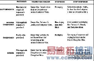
Figure 5: This figure shows a general frequency domain and time domain description of the more popular Butterworth, Chebyshev and Inverse Chebyshev filters.
Keep dc signals clean
The easiest implementation of an anti-aliasing filter design is for a circuit that has a dc sensor. With this type of system, the low-pass filter primarily reduces circuit noise. The attenuation of frequencies that may cause aliasing problems is usually not an issue because they occur at frequencies well above the corner frequency of the filter. Figure 6 shows a sensor circuit that produces a dc output.
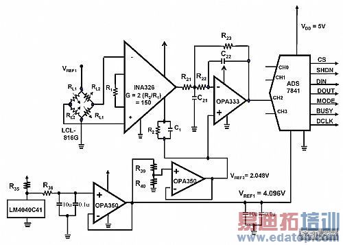
Figure 6: This load-cell sensing circuit converts the sensor’s differential response to weight into a voltage. This configuration uses TI’s INA362, an instrumentation amplifier, to differentiate the sensor signal. The signal is then filtered with the amplifier configuration of TI’s OPA333, R21, R22, R23, C2 1 and C22.
In order to reduce amplifier and conducted noise, the low-pass filter in this circuit has a cut-off frequency that is as low as possible. This circuit uses a Chebyshev filter with a 0.5 dB ripple because of the filter’s fast transition region in the frequency domain. The closest expected high frequency noise in this circuit is 60 Hz. The attenuation of this filter at 60 Hz is 27.3 dB down from dc.
If this circuit did not have the second-order low-pass filter in the signal path, the peak-to-peak voltage noise from TI’s instrumentation amplifier, INA326, would be 1.10 mVrms and 7.3 mVp-p at the input to the ADS7841 (quad 12-bit A/D converter). The LSB size of the 12-bit converter equal to:
ADCLSB = VREF/212
= 4.096V/4096
= 1 mV
This level of noise would produce a little less than 3-codes of noise, affecting the last two LSBs of all conversions. When using a second-order 10-Hz low-pass filter in this circuit, the peak-to-peak noise at the input of TI’s OPA333 changes to 0.32mV, which is well below the LSB threshold of the converter.
Multiplexing dc signals changes the filtering strategy
The anti-aliasing filter in Figure 7 must respond quickly to steps caused by the multiplexed circuit. Initially, it is tempting to select a filter that has a fast transition region in the frequency domain, but the group delay of these types of filters performs with a significant ringing in the time domain.
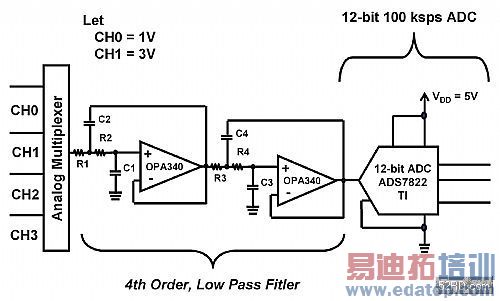
Figure 7: DC signals at the input of CH0-CH3 appear as a step response to the low-pass filter (OPA340s) after the multiplex switches from channel to channel. Given this type of input, the 12-bit A/D converter must wait for the filter to settle to its final value before the conversion.
A Bessel filter design is most appropriate for this application problem (Figure 7). Since the group delay of the Bessel is linear with change in frequency, the harmonics of the step response propagates through the filter so that there is a minimal amount of overshoot and ringing. This fourth-order Bessel filter has a smaller transition band than the second-order Chebyshev filter and it settles to 12-bit accuracy quicker.
Some circuits require a filter with a good combination of both
Sensors that operate at higher frequencies usually require a different filter solution than the ones presented previously. Figure 8 shows an example of an application that requires a filter that is relatively stable in the time domain and has good high frequency noise reduction.
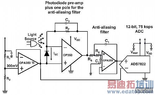
Figure 8: Many times, the filter for a photo-sensing circuit needs to have noise-reduction capability as well as a well-behaved time response. In this circumstance, the middle-of-the-road Butterworth filter is the best choice.
This type of circuit noise reduction in the frequency domain, as well as minimal ringing in the time domain, is critical. As shown previously, the Chebyshev filter has the smallest transition band. At first glance, this makes it a good candidate for this circuit until the time domain response is examined. Unfortunately, the group delay of the frequencies above the cut-off frequency of the Chebyshev filter can cause a considerable amount of ringing, hence signal contamination.
The alternative is the Bessel filter which has a well-behaved time response. However, if noise reduction is a crucial part of the circuit requirements, the order of the Bessel filter may need to be unreasonably high. A good compromise to this problem is to use the Butterworth filter. This middle of the road solution often services the application by reducing noise with minimal ringing and, most importantly, with as few amplifiers, resistors and capacitors as possible.
Conclusion
It is tempting to use only a digital filter to reduce noise in the analog signal path or to completely go without the filter. The digital filter serves a useful function by being easily programmable without expensive hardware modifications. Otherwise, the analog filter is a critical element in mixed signal applications. In the absence of an analog, low-pass filter, noise is easily aliased back into the resulting A/D conversion.

