- 易迪拓培训,专注于微波、射频、天线设计工程师的培养
低压降稳压器、SMPS 级联可抑制纹波、保持高效率(英)
A step-down SMPS (switched-mode power supply) efficiently converts unregulated power to a regulated output voltage. However, unwanted switching-induced ripple and input transients may appear on the output. Applying noisy power to an RF power amplifier can inject spurious signals or modulated noise into the broadcast spectrum. Analog- and RF-system engineers favor traditional low-noise power-supply designs that comprise a transformer, rectifier, and filter followed by a linear voltage regulator. A low-dropout linear regulator’s low output noise and high PSRR (power-supply rejection ratio) ensure clean power that imposes no interference on a power amplifier’s output.
Unfortunately, a transformer-and-rectifier power supply delivers a fluctuating output voltage that depends on its input voltage. As the difference between its input and output voltage increases, a low-dropout regulator’s efficiency decreases, and its power dissipation increases. To remain in regulation at low ac-line voltages, even a low-dropout regulator requires a certain amount of head-room input-to-output voltage.
To overcome the disadvantages inherent in both circuits, you can use an SMPS to maintain high efficiency and a low-dropout regulator to reduce the output noise and ripple voltage of the SMPS. Setting the output voltage of the SMPS slightly higher than the low-dropout regulator’s minimum dropout voltage reduces the regulator’s power dissipation, accommodates the voltage margin you need for good switching-noise rejection, and maintains high efficiency. The regulators’ PSRRs add, and the combined circuits’ PSRR exceeds that of either the regulator or the SMPS alone.
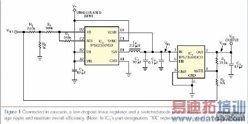
Figure 1 shows a cascade circuit comprising an SMPS followed by a linear regulator. This circuit’s output voltage ranges from 1.5 to 5V at an output current as high as 400 mA. Although a fixed 6V supply powers the cascaded circuit, its design accommodates any input voltage at least 0.5V higher than the cascaded pair’s desired output voltage.

Adjusting the reference voltage, VSET, over 0 to 1.105V linearly varies the circuit’s output voltage. Resistors R1 and R2 and reference voltage VSET determine the low-dropout regulator’s output voltage and thus the cascaded pair’s output voltage. Resistors RT, RB, R3, and R4 divide VSET to maintain the SMPS’ output voltage, VPS, at a constant 0.2V higher than the regulator’s output voltage, reducing the regulator’s power dissipation to 80 mW at full output current and any output voltage.
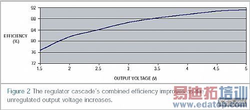
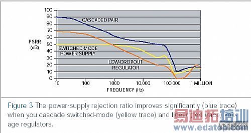
At its maximum output current of 400 mA, the cascaded supply reaches a maximum efficiency of 89% with a 6V input and a 4.69V output (Figure 2). The overall efficiency decreases as the output voltage decreases. Figure 3 compares the PSRRs of the SMPS alone and of the SMPS cascaded with the regulator, which improves PSRR by 46 dB at 500 Hz—essentially that of the regulator alone at 500 Hz.


Over a frequency range of 100 Hz to 100 kHz, the low-dropout regulator improves PSRR by at least 25 dB (Figure 3). Circuit-layout and -measurement techniques compound the difficulty of making accurate small-signal measurements, and the graph’s PSRR values may not appear additive. The linear regulator governs the circuit’s switched-load transient response, which may represent an improvement over the response of the SMPS. However, the cascade circuit’s low output ripple and high efficiency make the circuit well worth investigation.

