- 易迪拓培训,专注于微波、射频、天线设计工程师的培养
数据转换器突破性进展对 SDR 设计的支持作用(英)
ADC considerations
A high-IF architecture is desirable from a receiver-hardware commonality perspective, but it places an added burden on the analog-to-digital converter (ADC) for wide dynamic range, which is typically determined by the ADC’s performance in the system. In a cellular infrastructure, for example, receivers must process very low-level signals (<-100 dBm) in the presence of high-power blockers (–13 dBm or –26 dBm in the case of GSM 800/900 and 1800/1900, respectively). Thus, the ADC must have wide spurious-free dynamic range (SFDR) and SNR to meet the receiver’s needs for this protocol.
The ADC’s speed has a direct impact on the receiver’s implementation. Depending on the system’s IF, increasing the ADC’s sampling rate has the effect of increasing the signal’s oversampling ratio, or decreasing its undersampling ratio. Additionally, noise is spread over a wider bandwidth when using a higher-speed ADC. This factor can be exploited with precise frequency planning.
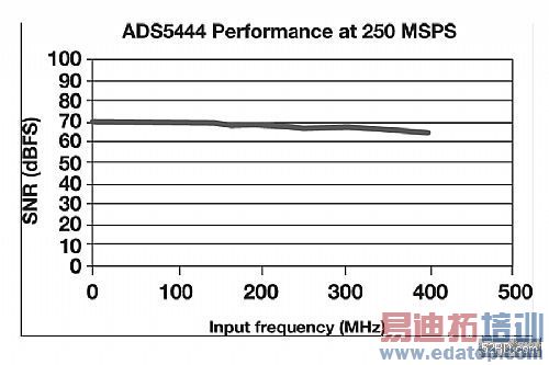
Consider two high-speed ADCs, one at a 100-Msample per second (MSPS) rate and the other at a 250-MSPS rate. Assuming both devices are specified to deliver 70 dBFS (fullscale) SNR, the effective noise contribution on a per-hertz (Hz) basis for the first ADC is –147 dBFS/Hz, while the faster one yields –151 dBFS/Hz, respectively. A frequency plan that allows for harmonic distortion products, which typically limit SFDR performance, may cause noise to fall outside of the bandwidth of interest. The reduced noise contribution of a higher-speed device can be exploited to allow for a higher-sensitivity receiver’s implementation This added benefit, often called the processing gain, is a fundamental advantage of using ADCs with very high sampling rates, such as the 13-bit, 250- MSPS ADS5444, Figure 1.

Figure 1: The combination of high SNR and high sample rate is a key consideration in ADC selection.
For high-IF implementations, an increased input bandwidth is also desirable, since it eases filtering requirements after the mixing process. An increase in IF frequency at the mixer’s output will place mixing products at an equivalent distance away from the bandwidth of interest. It is critically important, however, to understand the difference between the analog input bandwidth as typically specified in data sheets and the “useful” analog input bandwidth for the radio’s design.
The high-speed ADCs typically seen today can exhibit 3-dB analog input bandwidths that span several hundred megahertz, but the fall-off in linearity and noise renders the converter unusable at very high-input frequencies. Consequently, system designers should focus on the ADC’s actual performance (SFDR and SNR vs. input frequencies.)
A significant consideration for any high-speed communications system is the generation of ultralow-jitter, high-speed sampling clocks and their effect on the data conversion process. There are two basic components to this jitter: One originates from the external clock source; the ADC’s clock circuitry creates the other internally. All jitter sources add (in a root-sum-squares manner) and contribute to the overall system’s SNR degradation:

where fin is the incoming signal’s frequency to be sampled by the data converter, and tjitter is the sampling system’s rms jitter.
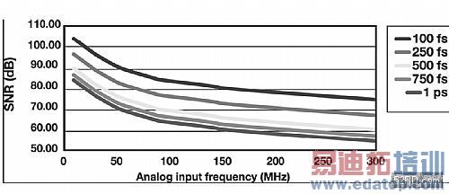
Figure 2 shows jitter’s effect on the system’s SNR performance.

Figure 2: Theoretically attainable SNR vs. input frequency for various RMS values of an overall system’s jitter.
For 70-dB SNR performance, with the clock’s rms and ADC’s jitter at 1 picosecond, the maximum frequency of the incoming signal cannot exceed 50 MHz. This assures that jitter effects will not limit receiver performance. Conversely, improving the clock’s jitter performance signal to 250 femtoseconds allows for 200-MHz IF usage while maintaining the same 70 dB of SNR performance. Careful selection of clock distribution components such as the CDCM7005 clock synchronizer and jitter cleaner ensures optimum performance from the ADC.
To optimize the transmitter’s performance and minimize cost, power-amplifier linearization schemes are becoming popular in the SDR transmitter designs. Digital pre-distortion algorithms require feedback paths with very wide bandwidth. This, in turn, mandates the use of ultrafast ADCs. Analog input-bandwidth “flatness” is also an important attribute in the right ADC selection. This is especially true in multicarrier systems, where several harmonics of the desired signal need to be digitized for effective power- amplifier linearization.
DAC considerations
Adding digital functionality in high-performance DACs provides an increased level of flexibility when implementing common IF schemes. Interpolation filters allow for sampling- rate increases in the digital domain while attenuating images created by the interpolation process result in an improved update rate-to-output frequency ratio for the DAC and more accurate waveform reconstruction. The trade-off with interpolation is the decrease of available signal bandwidth by a factor equal to the interpolation multiple; interpolating by a factor of 4 reduces the available signal bandwidth by 4.
Using fine (NCO-controlled) and coarse (fclk/n) digital mixers results in an increased degree of frequency-placement freedom while signals are still in the digital domain. But this process creates mixing products that must be filtered out of the analog domain. Sin(x)/x compensation allows for higher frequency placement, at the expense of slightly reducing power in the bandwidth of interest and SNR performance.
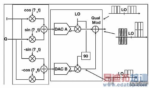
A complex IF architecture allows for quadrature signals, while it eases analog-domain filtering requirements. The presence of phase information during the mixing process permits the arithmetic cancellation of signals. This process dramatically reduces the power of mixing products, Figure 3.

Figure 3: Minimizing unwanted sidebands in a direct up-conversion transmitter.
When the mixing images are full power, their attenuation in a complex-IF implementation represents a significant advantage over real IF. Additionally, quadrature-correction circuitry in the digital domain effectively eliminates local oscillator (LO) feedthrough at the final RF and further reduces filtering needs.
Figures 4a, b, and c illustrates the performance achieved using a complex-IF implementation, using the RF output of a TI TSW3000 transmit-reference design.


Figures 4a, b, and c: Output spectra of TI’s TSW3000 transmit reference design, illustrating image suppression at various Fdac multiples (wanted carrier is centered at 2.14 GHz).
This enhancement was not done in this example, to more closely emulate an SDR implementation. The DAC’s built-in functionality, such as the DAC5687 used here, facilitates carrier optimization (LO) and sideband suppression.
An important function when implementing a true SDR system is the ability to perform baseband data-rate changes, without adjusting data-converter clocks. This resampling function, though not performed in the data converter itself, needs to be taken into account during the implementation phase. For systems handling multiple transmission protocols, the resampling circuitry provides an invaluable tool to simplify overall system design. The circuit allows the baseband data rate (post-channelization) to have a noninteger relationship with the input sample clock. It also allows for a common sample clock, while maintaining the ability to operate across multiple transmission protocols.

