- 易迪拓培训,专注于微波、射频、天线设计工程师的培养
选择 DC/DC 转换器的最佳开关频率(英)
Many power IC suppliers are aggressively marketing faster DC/DC converters that claim to save space. A DC/DC converter switching at 1 or 2 MHz sounds like a great idea, but there is more to understand about the impact to the power supply system than size and efficiency. Several design examples will be shown revealing the benefits and obstacles when switching at faster frequencies.
Selecting an Application
Three different power supplies were designed and built to show the trade offs of high switching frequency. For all three designs, the input voltage is 5V, the output voltage is 1.8V, and the output current is 3A. These requirements are typical for powering a performance processor such as a DSP, ASIC or FPGA. To bound the filter design and performance expectations, the allowable ripple voltage is 20 mV, which is about one percent of the output voltage, and the peak-to-peak inductor current is chosen at 1A.
Independent designs at frequencies of 350, 700, and 1600 kHz will be compared to illustrate the benefits and obstacles. The TPS54317, a 1.6 MHz, low-voltage, 3 A synchronous-buck DC/DC converter with integrated MOSFETs was chosen as the regulator in each example. The TPS54317 from Texas Instruments features a programmable frequency, external compensation and is intended for high-density processor power point-of-load applications.
Selecting the Inductor and Capacitor
The inductors and capacitors are chosen according to the following simplified formulas:
Equation 1:
V = L x di/dt
Rearranging: L ≥ Vout x (1-D)/(ΔI x Fs)
where: ΔI = 1 A peak-to-peak; D = 1.8 V/5 V=0.36
Equation 2:
I = C x dv/dt
Rearranging: C ≥ 2 x ΔI/(8 x Fs x ΔV)
where: ΔV = 20 mV, I = 1 A peak-to-peak
Equation 2 assumes a capacitor is used that has negligible series resistance, which is true for ceramic capacitors. Ceramic capacitors were chosen for all three designs because of their low resistance and small size. The multiplier of two shown above in the rearranged Equation 2 accounts for capacitance drop associated with DC bias, since this effect is not accounted for in the datasheets of most ceramic capacitors.
The circuit in Figure 1 was used to evaluate the performance of each design on the bench.
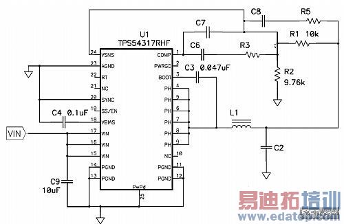
Figure 1: TPS54317 Reference Schematic.
The components in the schematic that do not have values are the components that were modified in each design. The output filter consists of L1 and C2. The values of these components for all three designs are listed in Table 1, and were chosen based on the results from the equations above.

Table 1: Capacitor and inductor selections at 350kHz, 700kHz, and 1600 kHz.
Note that the DC resistance of each inductor decreased as the frequency increased. This is due to less copper length needed for fewer turns. The error amplifier compensation components were designed independently for each switching frequency. The calculations for selecting the compensation values are beyond the scope of this article.
Minimum on-time
Digital converters-to-digital converter integrated circuits (IC) are characterized with a limit on the minimum controllable on-time, which is the narrowest achievable pulse width of the pulse width modulation (PWM) circuit. In a buck converter, the percentage of time that the field effect transistor (FET) is on during a switching cycle is called the duty cycle, and is equal to the ratio of the output voltage to input voltage.
For the converter example above, the duty cycle is 0.36 (1.8V/5.0V) and the minimum on-time of the TPS54317 is 150ns (max) as shown in the datasheet. The limit for the controllable pulse width results in a minimum achievable duty cycle, which can be easily calculated as shown in Equation 3. Once the minimum duty cycle is known, the lowest achievable output voltage can be calculated, as shown in Equation 4 and Table 2. The lowest output voltage is also limited by the reference voltage of the converter, which is 0.9V for the TPS54317.
Equation 3:
Minimum duty cycle =
Minimum on-time x Switching frequency
Equation 4:
Minimum Vout =
Vin x Minimum duty cycle (bounded by TPS54317 Vref)
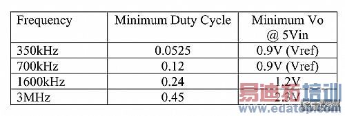
Table 2: Minimum output voltage with 150 ns minimum on-time.
In this example, a 1.8V output can be generated with a 1.6 MHz switching frequency. However, if the frequency is 3MHz, the lowest possible output voltage is limited to 2.3 V and the DC/DC converter will skip pulses. The alternative is to lower the input voltage or reduce the frequency. It is a good idea to check the DC/DC converter datasheet for a guaranteed minimum controllable on-time before selecting a switching frequency.
Pulse Skipping
Pulse skipping occurs when the DC/DC converter cannot extinguish the gate drive pulses fast enough to maintain the desired duty cycle. The power supply will try to regulate the output voltage, but the ripple voltage will increase due to the pulses being further apart. Due to the pulse skipping, the output ripple will exhibit sub-harmonic components, which may present noise issues. It is also possible that the current limit circuit will no longer work properly since the IC may not respond to a large current spike. In some cases, the control loop may be unstable since the controller is not performing properly. The minimum controllable on-time is an important attribute and it is wise to check the DC/DC converter’s specification in the datasheet to verify a frequency and minimum on-time combination.
Efficiency and Power Dissipation
The efficiency of a DC/DC converter is one of the most important attributes to consider when designing a power supply. Poor efficiency translates into higher power dissipation which has to be managed on the circuit board with heat sinks or additional copper on the printed circuit board. Power dissipation also places a higher demand on the power supply upstream. Power dissipation has several components shown below:

The loss components of interest from our three examples come from the FET driving loss, the FET switching loss and the inductor loss. The FET resistance and IC loss are consistent since the same IC is used in all three designs. Since ceramic capacitors were chosen in each example, the capacitor loss is negligible due to their low equivalent series resistance. To show the effects of high frequency switching, the efficiency of each example was measured and illustrated in Figure 2.
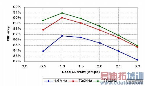
Figure 2: Efficiency at 5 V input and 1.8 V output at various frequencies.
The figure clearly shows that the efficiency is decreased as switching frequency is increased. To improve efficiency at any frequency, look for a DC/DC converter with a low Rds (on), gate charge, or quiescent current specification at full load, or search for capacitors and inductors with lower equivalent resistance.
Size
Table 3 shows the inductor and capacitor values with the pad area required on the printed circuit board.

Table 3: Component size and total area requirements
The recommended pad area of a capacitor or inductor is slightly larger than the individual component itself, and the pad area dimension is accounted for in each of the three design examples. Then, the total area was derived by adding the area occupied by each component, which includes the pad sizes for the IC, the filter and all other small resistors and capacitors multiplied by a factor of two to account for component spacing. The total area savings from 350 kHz to 1600 kHz is significant and provides a 50 percent reduction in filter size and a 35 percent reduction in board space, saving almost 100mm2.
However, the law of diminishing returns applies since the capacitance and inductance values cannot be reduced to nothing! In other words, pushing the frequency higher will not continually reduce the overall size since there is a limitation to appropriately sized mass produced inductors and capacitors.
Transient Response
The transient response is a good indicator of the performance level of a power supply. A Bode plot of each power supply was taken to show a comparison at higher switching frequencies. As shown in Figure 3, the phase margin of each power supply is between 45 and 55 degrees, indicating a well-dampened transient response.
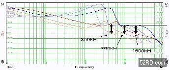
Figure 3: Bode plots at 350 kHz, 700 kHz, and 1600 kHz.
The cross over frequency is approximately one-eighth of the switching frequency. When using a fast switching DC/DC converter, make sure the power IC error amplifier has enough bandwidth to support a high crossover frequency. The TPS54317 error amplifier unity gain bandwidth is typically 5MHz. The actual transient response times are shown in Table 4 with the associated voltage peak overshoot value.

Table 4: Transient response.
The overshoot value is significantly lower with the higher switching frequency, due to the wider bandwidth. Lower transient voltage overshoots are desirable with newer performance processors as their regulation accuracy requirement may be three percent including transient voltage peaks.
When higher output currents are needed, Texas Instruments offers the TPS40140 stackable, dual-channel, 1 MHz DC/DC controller using external MOSFETs. The benefits of a fast switching frequency can be realized by interleaving a number of power stages and switching them out of phase.
For example, four outputs can be tied together switching at 500 kHz each, for an effective frequency of 2 MHz. The benefits are lower ripple, reduced input bulk capacitance, faster transient response, and better thermal management by spreading out the power dissipation over the circuit board. Up to eight TPS40140 devices can be connected and synchronized out of phase via digital bus for a maximum effective frequency of 16 MHz.
Summary
There are tradeoffs to designing high-frequency switching converters. Some of the advantages shown in this article are a smaller size, faster transient response and smaller voltage over and undershoots. On the other hand, the main penalty paid is a reduction of efficiency and increased heat dissipation.
There are potential pitfalls to pushing the envelope such as pulse skipping and noise issues. When selecting a DC/DC converter for high frequency applications, check the manufacturer’s datasheet for important specifications such as the minimum on-time, the gain-bandwidth of the error amplifier, the FET resistance and switching loss. Integrated circuits that perform well in these specifications will cost a premium, but will be worth the price and much easier to use when cornered with a tough design problem.
上一篇:《SAR 型与高速 ΔΣ 型 ADC 的选择》(英)
下一篇:数据转换器突破性进展对 SDR 设计的支持作用(英)

