- 易迪拓培训,专注于微波、射频、天线设计工程师的培养
Resistive tap monitors and sets W-CDMA power levels
The LMV225 is a 30dB RF power detector intended for use in CDMA and WCDMA cell phone applications. The device has an RF frequency range from 450MHz to 2GHz. It provides an accurate temperature and supply compensated output voltage that relates linearly to the RF input power in dBm. The circuit operates with a single supply from 2.7V to 5V. The LMV225 has an integrated filter for low-ripple average power detection of CDMA signals with 30dB dynamic range. Additional filtering can be applied using a single external capacitor.
The LMV225 has an RF power detection range from _30dBm to 0dBm and is ideally suited for direct use in combination with resistive taps. The device is active for Enable = HI, otherwise it goes into a low power consumption shutdown mode. During shutdown the output will be LOW. The output voltage ranges from 0.2V to 2V and can be scaled down to meet ADC input range requirements. The output signal bandwidth can optionally be lowered externally as well.
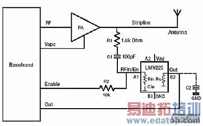
A typical control loop application with LMV225 is depicted in Figure 1. The output of the power amplifier is connected to the RF input of the power detector, while the output of the detector is connected to the base band chip. The baseband chip adjusts the gain of the PA by its Vapc pin (if needed) to set the correct PA output power. The power detector is especially suited for measurements via a high-resistive tap, which is a low cost alternative for a directional coupler.
The LMV225 can be used in conjunction with PAs like National''s LP3939, an integrated device that provides interface to the baseband processor to powerswitch two independent power amplifiers in dual band applications (particularly, in Qualcomm- compatible phones. By integrating the discrete components necessary to achieve the same functions, the LP3939 drastically reduces board space and component cost.
This article describes the operating principles of the power detector as well as the configuration of a typical application. The attenuation required between the PA and the LMV225 is calculated and confirmed by measurement. Important in this application is also the output ripple of the detector, which can be reduced by adding a capacitor.
Power detector
The DC output voltage of the power detector is a measure for the amount of power on its input. Its output voltage is linear with the logarithm of the input power in dBm. This is often called a linearin- dB response. The logarithmic response makes the calibration process easy.
A de-modulating logarithmic amplifier as depicted in Figure 2 implements the logarithmic function in the detector. The logarithmic amplifier consists of a number of cascaded linear gain cells. With these gain cells, a piecewise approximation of the logarithm is constructed. All gain cell outputs (X1 to X3) as well as the input signal X0 are AM demodulated with peak detectors and summed together. This implements the logarithmic function (Y).
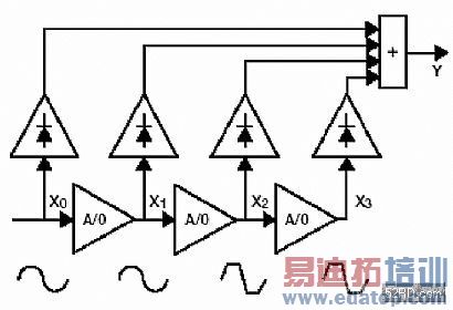
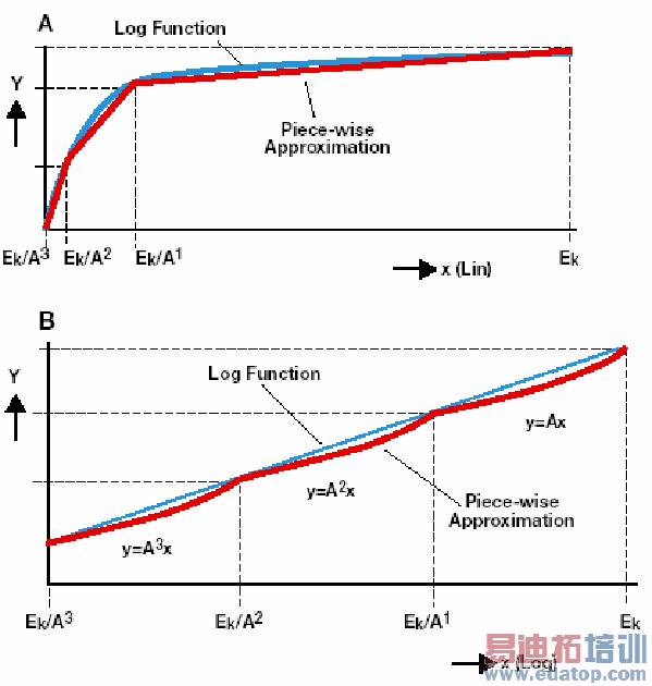
The gain cells used in the LMV225 are called "A/0"-gain cells and have a response according to Figure 3. The output (Y) is the input (X) multiplied by a certain gain (A) until the threshold voltage EK is reached. The gain cell saturates after this threshold is reached. Several gain cells are connected to each other, where the output of one gain cell is connected to the input of the next gain cell. The signal is amplified sequentially through the gain cells until it exceeds the threshold (EK). The particular gain cell saturates and consequently all the following gain cells will not amplify the signal anymore. The minimum logarithmic range of the detector is the number of gain cells times their gain in dBm. Figure 4a and 4b show a logarithmic function and its piecewise approximation implemented in the LMV225, where Ek/A3 to Ek are threshold voltages of each of the gain cells. The resulting function Y is the logarithmic function of the input X.
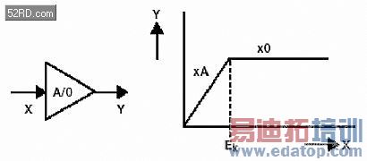
Figure 4a simultaneously depicts the logarithmic function and the implemented piecewise linear approximation. 4b shows the same data on a log-scale.
Piecewise approximation of logarithmic in practice
The LMV225 has 3 gain cells with a gain of 10 dB each. The logarithmic range is therefore 30dB although the range is larger in practice. This is because the gain cells have smoother gradual transitions then theoretical assumed in Figure 3. Error! Reference source not found.5 (the blue curve) shows a typical detection curve of the LMV225 at 900MHz.
The detection curve looks linear at first sight, but when the detection curve is compared with a logarithmic function the log conformance error is seen. This error is due to the piecewise approximation of the logarithmic function. The difference in dB between the ideal logarithmic and the detection curve at a certain output voltage is displayed. The log conformance response doesn''t show the sharp saturation point EK from the response of Figure 3. This is because a gain cell saturates smoothly instead of abrupt. It has a more curved response. The error stays within +/" 1 dB from the ideal logarithmic function over an input range of 40 dB. This is generally enough accuracy to do a reliable measurement for the application.
Attenuation
The dynamic range of the PA output and the detector input don''t match. In order to match these ranges, attenuation has to be placed between PA and RF input. This can be implemented with a high resistive tap solution. Resistor R1 (high resistive tap) and the 50-ohm input resistance of the device realize the attenuation (Figure 1). The constant input impedance of the LMV225 enable the realization of a frequency independent input attenuation. To minimize insertion loss and not disturb the strip line characteristics, resistor R1 needs to be sufficiently large. The value of resistor R1, to obtain the correct attenuation, can be calculated easily. The attenuation is a resistive divider formed by R1 and the input impedance RIN of the LMV225.
In Figure 1, R1 is set to a standard value of 1800 ohms resulting in an attenuation of 31.4 dB. Special care should be taken by choosing a resistor with a sufficient bandwidth. Otherwise the attenuation is less and it can cause non-linearity.
To minimize the number of pins and thereby the dimension of the package of the IC, the shutdown and the power detection are combined into one pin. The capacitor C1 and the resistor R2 in Figure 1 separate the DC shutdown functionality from the AC power measurement. The device is active when Enable = HI, otherwise it goes into shutdown. During shutdown the output is LOW.
Capacitor C1 should be chosen sufficiently large to ensure a corner frequency far below the lowest input frequency to be measured. Where RIN = 50- ohms, CIN = 45 pF typical. With R1 = 1800 ohms and C1 is 100pF, this results in a corner frequency of 2.8MHz.
Figure 5 shows the typical curve of the detector''s output as a function of the output of the PA
Figure 5: Typical power detector response, VOUT vs. Power.
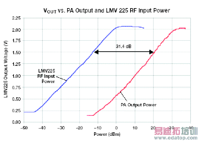
and the RF input of the detector. The setup used for this measurement is depicted in Figure 1. It can be seen that the attenuation of 31.4 dB is achieved. The response is linear in dB''s.
Output Ripple due to AM Modulation
Until now we assumed that the RF signal is constant. A CDMA modulated carrier wave generally contains some amplitude modulation that might disturb the RF power measurement. The relation between the amplitude modulation in the RF signal and the ripple on the detector''s output due to this modulation can be estimated. The ripple can be reduced by connecting an additional capacitor to the output of the LMV225 to ground.
In operation, the ripple is independent of the average input power of the RF input signal and only depends on the logarithmic slope VY and the ratio of the maximum and the minimum input signal amplitude. A further understanding can be achieved via the knowledge that the transfer from the RF input to the output of the LMV225 is linear in dB For CDMA, the ratio of the maximum and the minimum input signal amplitude modulation is typically in the order of 5 to 6 dB, which is equivalent to a modulation index of 0.28 to 0.33.
The variation observed on the output (delta-VOUT) consists of the ripple due to AM modulation and the log-conformance error. The log-conformance error is usually much smaller than the ripple due to AM modulation and is therefore neglected. In case of the LMV225, Vy = 40mV/dB. With delta-PIN = 5dB, the delta-VO = 200mVPP.
The calculated result above is for an unfiltered configuration. When a low pass filter is used by shunting a capacitor of e.g. C2 = 1.5nF at the output of the LMV225 to ground (Figure 1), this ripple is further attenuated.
With the output resistance of RO = 19.8k ohms typical (LMV225 datasheet) and C2 = 1.5nF, the cutoff frequency fC equals 5.36kHz. A 100kHz AM signal then gets attenuated by 25.4dB. The remaining ripple will be less than 11mV. With a slope of 40mV/dB this translates into an error of approximately 0.25dB on the RF input. If the capacitor value C2 is chosen to high, it will reduce the rise time of the detector.
Ripple reduction can be achieved by adding additional capacitance on the output of the LMV225. The RF signal of 900MHz is AM modulated with a 100kHz sine wave and a modulation index of 0.3. The RF input power is swept while the modulation index remains unchanged. Without addition capacitance the ripple is about 200mVPP. Connecting a capacitor (1.5nF) results in a ripple of 12mVPP, which is an attenuation of 20log (200/12) = 24.4dB. This is close to the predicted value. --

