- 易迪拓培训,专注于微波、射频、天线设计工程师的培养
Linear Power Control Of GSM Amplifier Power (2)
Once the slope and the intercept are known, the required code for any transmit power level can be calculated using the formula:

The RF power-detection method suffers only ? dB error for an output-power range spanning +5 to +34.5 dBm, while the current-sensing and voltage-sensing methods exhibit higher errors for narrower power levels.
The RF power-detection approach uses an internal 30-dB coupler. Because of this low coupling factor, the insertion loss of this coupler is extremely low (approximately 0.05 dB), and has a minimal impact on PA efficiency. This impact can be described by a loss factor of 10−0.05/10. The PAE of the amplifier module is then the PAE of the amplifier integrated circuit (IC) multiplied by this loss factor. It should be noted that all PAE specifications for the RF power-detection approach include the effect of directional coupler insertion loss.
The FET used in the voltage-sensing approach has a voltage drop of about 180 mV at full power. This will also reduce the efficiency of PA chip inside the module. This loss in efficiency is approximately:

This loss factor is similar to the RF power-detection approach at nominal supply voltages. However, it is worse at low supply voltages. Amplifier module PAE specifications for the voltage-sensing approach also include the PAE loss due to the FET.
The log detector controller has a control function that is linear when scaled in dB/V. To achieve the desired raised-cosine RF power profile from the PA, the ramping signal from the ramp DAC should also follow a raised-cosine form.
During initialization and completion of the transmit sequence, the PA bias voltage should be held at its minimum level by keeping the external control voltage at some level below 150 mV (this is generally achieved by setting the ramp DAC code to 0). The PA has a clamping mechanism designed to keep the PA off, with high isolation, when the VSET voltage is below 150 mV.

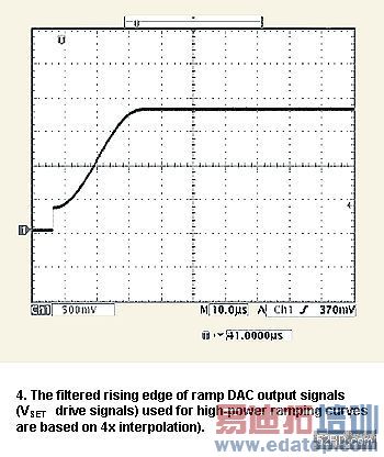
To optimize switching transients a step is applied to the ramp (Fig. 4). The step is used because there is no point in ramping from 0 to 200 mV because the PA is designed to stay off for this voltage range.
When ramping to lower power levels, the same initial offset voltage should be applied before ramping begins. The raised-cosine portion of the ramp should be scaled to set the desired power level. The ramp-down profile can be a simple mirror image of the ramp-up signal (i.e., the same codes can be used). Alternatively, the ramp DAC signal can be a simple raised-cosine signal that falls all the way to 0 V. This is not true for the voltage-sensing and current-sensing control methods. These methods require more than one ramp profile, especially at low power levels, in order to achieve good ramping and switching transients.
A filter (CFLT and RFLT) must be used to stabilize the loop and ensure optimum conformance to the time mask and switching transient specifications (as shown in Fig. 2). The choice of CFLT and RFLT will depend to a large degree on the gain-control dynamics of the PA. The optimum values for the control loop have been determined to be 220 pF for the capacitor and 3 k?for the series resistor for GSM and 4.3 k?and 150 pF for the resistor and capacitor, respectively, in DCS/PCS systems. This gives the loop sufficient speed to follow the required ramping profiles, while still meeting the switching transient requirements at all power levels. Depending on the board layout and choice of transmit components, these values may have to be adjusted slightly. Generally, meeting these requirements is most difficult at full power.
上一篇:Antenna Measurement Techniques (1)
下一篇:Linear Power Control Of GSM Amplifier Power (一)

