- 易迪拓培训,专注于微波、射频、天线设计工程师的培养
RF Power Reduction for CDMA/W-CDMA Cellular Phones
To meet the stringent specifications for linearity and adjacent-channel power ratio (ACPR) found in the IS95/3GPP spread-spectrum standard, CDMA/W-CDMA1 wireless handsets require highly linear Class-A or Class-AB RF power amplifiers. The power-added efficiency (PAE) for that type of PA, however, is only about 35% maximum at Po = 28dBm, and much lower for lower power levels.
The PA does not operate continuously in voice mode. When the phone user isn''t speaking, it runs at half rate (50% of the time) or at one-eighth rate, so there is no worry about the phone heating up during voice mode. In data mode, however, the PA runs continuously until the data transmission is complete. The combination of low PA efficiency and continuous PA operation causes the battery to drain quickly, and the resulting internal power dissipation can also make the phone overheat.
Power dissipation was a major problem for the early W-CDMA handsets that supported high-speed data-transmission services. It forced designers to include larger area heat sinks, more airflow for cooling, and larger capacity (bigger) batteries. Had they not overcome the issue of power dissipation, today''s handsets would be bulky and heavy. Fortunately, the past few years have alleviated this problem by providing a dramatic improvement in PA power efficiency for CDMA/W-CDMA cell phones.
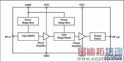
How to Reduce PA Power? As shown in Figure 1, two supply voltages are required for the CDMA/W-CDMA power amplifier. VREF provides bias for the internal driver and power-amplifier stages, and VCC biases the collectors for the driver and power amplifiers. The PA supply current can be reduced by adjusting those two voltages.
In CDMA/W-CDMA systems, the PA''s RF power output is not always at maximum. To optimize the cell capacity (number of simultaneous transmissions that a base station can handle), each mobile phone controls its RF output power such that the effective signal-to-noise level received at the base station is the same for each phone. A probability distribution of the RF output-power levels from many phones in a given area shows that the average output power from a typical CDMA/W-CDMA phone is about +10dBm for suburban conditions and about +5dBm for urban conditions. Thus, a useful target for improving PA efficiency is not the maximum power level, but an approximate range of +5dBm to +10dBm. 
Figure 1. A typical power amplifier for CDMA/W-CDMA cell phones.
Reducing VREF
When transmitting zero RF power, the PA itself draws a typical quiescent current of 100mA at VREF = 3.0V and VCC = 3.4V. Reducing VREF from 3.0V to 2.9V causes the quiescent current to drop about 20mA. Thus, a dramatic savings can be achieved in PA quiescent current by lowering VREF, but not below the point at which the PA linearity and ACPR begin to fail their specifications.
If there is experimental data giving the minimum VREF voltage required to support each output-power level slotted for the PA, one can actively couple the control of VREF with the PA''s power-control process. If that approach is too difficult, one can simply implement a two-step change in VREF that corresponds to the low-power mode (<10dBm) and high-power mode (>10dBm). To adjust VREF via the baseband control DAC, use a low-power op amp with high output-current capability, along with an external gain setting.
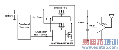
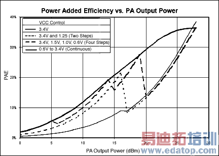
Reducing the Collector-Bias Voltage A variable bias voltage for the PA collector is provided by a specially designed, high-efficiency DC-DC stepdown converter. The output voltage of this converter is adjusted using a dedicated DAC output from the baseband processor. DC-DC Converter Controls PA Power and PAE Connecting the DC-DC converter between the PA and battery highlights a problem—the demand for high RF power at low battery voltage. To deliver 28dBm RF power while maintaining the specification for PA linearity, PA manufacturers recommend a minimum VCC of 3.4V. To maintain a 35% PAE at 3.4V, one also needs a high PA-collector current of 530mA: In this case (battery voltage below 3.665V), it is better to short the PA collector to the battery. Otherwise, one cannot access the full capacity of the Li-ion battery. Normally, the solution is to bypass the inductor and internal P-FET by connecting a low-Rds(on) P-FET in parallel. This bypass P-FET (which can be internal or external) connects battery voltage directly to the PA collector when in the high-power mode (Figure 2). For the combination of high RF power and low battery voltage, this bypass measure is a must-do. The very best method for optimizing PAE is to adjust the PA-collector bias continuously. That approach, however, requires factory calibration and sophisticated software that ensures good PA linearity and ACPR in the presence of continuously changing collector bias. The next best approach is to change the bias level in a series of steps, usually two to four (Figure 3). A four-step system, for instance, might consist of VCC values Vbatt, 1.5V, 1.0V, and 0.6V. The overall efficiency in such a system is nearly as good as that for a system with continuous control of the PA collector bias, and for low- and mid-power levels the inductor needs only to support peak currents of less than 150mA. Notes
In typical wireless handsets, the PA VCC is delivered directly from a single-cell Li-ion battery, resulting in an operating VCC range of 3.2V to 4.2V. As mentioned above, statistics show that the CDMA/W-CDMA PA operates at power levels of +5dBm to +10dBm most of the time. At those levels one can reduce the PA collector bias voltage (VCC) considerably without losing linearity in the PA, and at the same time reduce the power loss from excessive collector-bias headroom. Based on experimental tests at low power levels, one can maintain proper communications with the base station while lowering the PA collector bias all the way down to 0.6V.
The DC-DC converter controlling the PA collector voltage must respond quickly to a control signal. Usually, the converter''s output voltage should settle to within 90% of its new target voltage within 30ms following a change in analog control voltage from the baseband processor. The converter chip provides an appropriate internal gain between its VCC-control input and the output voltage that biases the PA collector. It also switches at high frequency, reducing the physical size of the inductor. 28dBm RF power: 102.8 mW = 631mW
To support a 3.4V VCC and 530mA ICC, the DC-DC converter for PA power requires a certain amount of input-to-output headroom. If, for example, on-resistance for the converter''s internal p-channel MOSFET (P-FET) is 0.4
Required PA power (VCC x ICC): 631mW/(PAE?00) = 1803mW
Required PA ICC at 3.4V VCC: ICC = 1803mW/3.4V = 530mA  and the inductor resistance is 0.1
 , the voltage drop across those two components in series will be (0.4
 +0.1
+0.1 ) x530mA = 265mV. Thus, the DC-DC converter is unable to support a 3.4V output when the battery voltage drops below 3.665V.
Figure 2. A DC-DC converter (middle IC) allows the baseband processor to exercise tight control over VCC for the power amplifier. 
Figure 3. A DC-DC converter provides maximum power-added efficiency (PAE) for the power amplifier shown in Figure 2.
1Code Division Multiple Access/Wideband Code Division Multiple Access
上一篇:高效匹配的小功率线性RF (射频)功率放大器
下一篇:Antenna Measurement Techniques (1)

