- 易迪拓培训,专注于微波、射频、天线设计工程师的培养
Virtex-6 FPGA ML605开发评估技术方案
录入:edatop.com 点击:
Virtex-6 FPGA适合用有线通信,无线基础设备和广播设备等领域.本文介绍了Virtex-6 FPGA主要特性,以及骨干网OTU-4成帧与EFEC框图, LTE 2x2无线电设计框图和支持SD/HD/3G-SDI接口的新一代交换框图, Virtex®-6 FPGA ML605评估套件主要特性和详细电路图.
The Virtex®-6 family provides the newest, most advanced features in the FPGA market. Virtex-6 FPGAs are the programmable silicon foundation for Targeted Design Platforms that deliver integrated software and hardware components to enable designers to focus on innovation as soon as their development cycle begins. Using the third-generation ASMBL™ (Advanced Silicon Modular Block) columnbased architecture, the Virtex-6 family contains multiple distinct sub-families. This overview covers the devices in the LXT, SXT, and HXT sub-families. Each sub-family contains a different ratio of features to most efficiently address the needs of a wide variety of advanced logic designs. In addition to the high-performance logic fabric, Virtex-6 FPGAs contain many built-in system-level blocks. These features allow logic designers to build the highest levels of performance and functionality into their FPGA-based systems. Built on a 40 nm state-of-theart copper process technology, Virtex-6 FPGAs are a programmable alternative to custom ASIC technology. Virtex-6 FPGAs offer the best solution for addressing the needs of high-performance logic designers, high-performance DSP designers, and high performance embedded systems designers with unprecedented logic, DSP, connectivity, and soft microprocessor capabilities.
Virtex-6 FPGA 主要特性:
• Three sub-families:
• Virtex-6 LXT FPGAs: High-performance logic with advanced serial connectivity
• Virtex-6 SXT FPGAs: Highest signal processing capability with advanced serial connectivity
• Virtex-6 HXT FPGAs: Highest bandwidth serial connectivity
• Compatibility across sub-families
• LXT and SXT devices are footprint compatible in the same package
• Advanced, high-performance FPGA Logic
• Real 6-input look-up table (LUT) technology
• Dual LUT5 (5-input LUT) option
• LUT/dual flip-flop pair for applications requiring rich register mix
• Improved routing efficiency
• 64-bit (or two 32-bit) distributed LUT RAM option per 6-input LUT
• SRL32/dual SRL16 with registered outputs option
• Powerful mixed-mode clock managers (MMCM)
• MMCM blocks provide zero-delay buffering, frequency synthesis, clock-phase shifting, inputjitter filtering, and phase-matched clock division
• 36-Kb block RAM/FIFOs
• Dual-port RAM blocks
• Programmable
- Dual-port widths up to 36 bits
- Simple dual-port widths up to 72 bits
• Enhanced programmable FIFO logic
• Built-in optional error-correction circuitry
• Optionally use each block as two independent 18 Kb blocks
• High-performance parallel SelectIO™ technology
• 1.2 to 2.5V I/O operation
• Source-synchronous interfacing using ChipSync™ technology
• Digitally controlled impedance (DCI) active termination
• Flexible fine-grained I/O banking
• High-speed memory interface support with integrated write-leveling capability
• Advanced DSP48E1 slices
• 25 x 18, two’s complement multiplier/accumulator
• Optional pipelining
• New optional pre-adder to assist filtering applications
• Optional bitwise logic functionality
• Dedicated cascade connections
• Flexible configuration options
• SPI and Parallel Flash interface
• Multi-bitstream support with dedicated fallback reconfiguration logic
• Automatic bus width detection
• System Monitor capability on all devices
• On-chip/off-chip thermal and supply voltage monitoring
• JTAG access to all monitored quantities
• Integrated interface blocks for PCI Express® designs
• Compliant to the PCI Express Base Specification 2.0
• Gen1 (2.5 Gb/s) and Gen2 (5 Gb/s) support with GTX transceivers
• Endpoint and Root Port capable
• x1, x2, x4, or x8 lane support per block
• GTX transceivers: up to 6.6 Gb/s
• Data rates below 480 Mb/s supported by oversampling in FPGA logic.
• GTH transceivers: 2.488 Gb/s to beyond 11 Gb/s
• Integrated 10/100/1000 Mb/s Ethernet MAC block
• Supports 1000BASE-X PCS/PMA and SGMII using GTX transceivers
• Supports MII, GMII, and RGMII using SelectIO technology resources
• 2500Mb/s support available
• 40 nm copper CMOS process technology
• 1.0V core voltage (-1, -2, -3 speed grades only)
• Lower-power 0.9V core voltage option (-1L speed grade only)
• High signal-integrity flip-chip packaging available in standard or Pb-free package options
Virtex®-6 FPGA典型应用: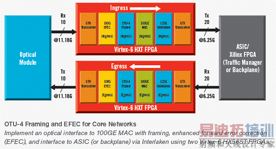
图1.骨干网OTU-4成帧和EFEC框图(有线通信)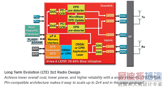
图2. LTE 2x2无线电设计框图(无线基础设备)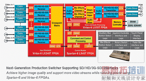
图3.支持SD/HD/3G-SDI接口的新一代交换框图(广播通信)
[p]
Virtex®-6 FPGA ML605评估套件
The Virtex®-6 FPGA ML605 Evaluation Kit provides a development environment for system designs that demand high-performance, serial connectivity and advanced memory interfacing. The ML605 is supported by pre-verified reference designs and industry-standard FPGA Mezzanine Connectors (FMC) which allow scaling and customization with daughter cards. Integrated tools help streamline the creation of elegant solutions to complex design requirements.
The ML605 board enables hardware and software developers to create or evaluate designs targeting the Virtex®-6 XC6VLX240T-1FFG1156 FPGA.
The ML605 provides board features common to many embedded processing systems. Some commonly used features include: a DDR3 SODIMM memory, an 8-lane PCI Express® interface, a tri-mode Ethernet PHY, general purpose I/O, and a UART. Additional user desired features can be added through mezzanine cards attached to the onboard high-speed VITA-57 FPGA Mezzanine Connector (FMC) high pin count (HPC) expansion connector, or the onboard VITA-57 FMC low pin count (LPC) connector.
This information includes:
• Current version of this user guide in PDF format
• Example design files for demonstration of Virtex-6 FPGA features and technology
• Demonstration hardware and software configuration files for the System ACE™ CF controller, Platform Flash configuration storage device, and linear flash chip
• Reference design files
• Schematics in PDF and DxDesigner formats
• Bill of materials (BOM)
• Printed-circuit board (PCB) layout in Allegro PCB format
• Gerber files for the PCB (Many free or shareware Gerber file viewers are available on the internet for viewing and printing these files.)
• Additional documentation, errata, frequently asked questions, and the latest news
Virtex®-6 FPGA ML605评估套件主要特性:
The ML605 provides the following features:
• 1. Virtex-6 XC6VLX240T-1FFG1156 FPGA
• 2. 512 MB DDR3 Memory SODIMM
• 3. 128 Mb Platform Flash XL
• 4. 32 MB Linear BPI Flash
• 5. System ACE CF and CompactFlash Connector
• 6. USB JTAG
• 7. Clock Generation
♦ Fixed 200 MHz oscillator (differential)
♦ Socketed 2.5V oscillator (single-ended)
♦ SMA connectors (differential)
♦ SMA connectors for MGT clocking
• 8. Multi-Gigabit Transceivers (GTX MGTs)
♦ FMC - HPC connector
♦ FMC - LPC connector
♦ SMA
♦ PCIe
♦ SFP Module connector
♦ Ethernet PHY SGMII interface
• 9. PCI Express Endpoint Connectivity
♦ Gen1 8-lane (x8)
♦ Gen2 4-lane (x4)
• 10. SFP Module Connector
• 11. 10/100/1000 Tri-Speed Ethernet PHY
• 12. USB-to-UART Bridge
• 13. USB Controller
• 14. DVI Codec
• 15. IIC Bus
♦ IIC EEPROM - 1 KB
♦ DDR3 SODIMM socket
♦ DVI CODEC
♦ DVI connector
♦ FMC HPC connector
♦ FMC LPC connector
♦ SFP module connector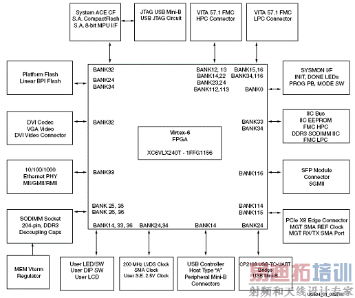
图4.ML605和外设框图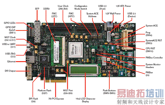
图5.ML605板外形图 [p]
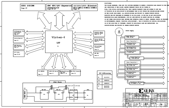
图6.ML605电路图(1)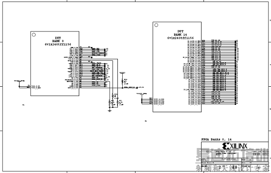
图7.ML605电路图(2)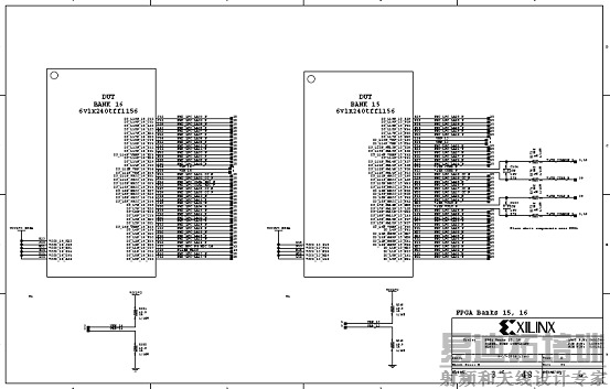
图8.ML605电路图(3)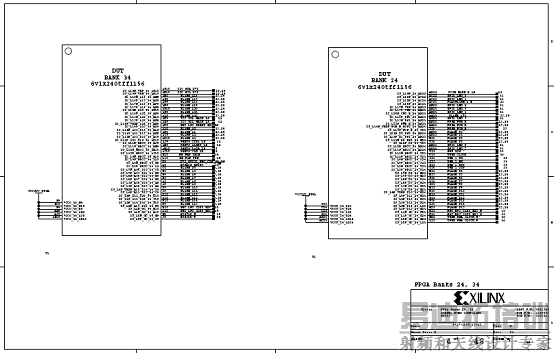
图9.ML605电路图(4)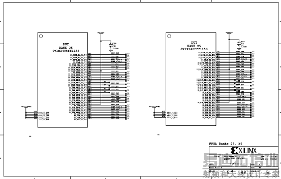
图10.ML605电路图(5)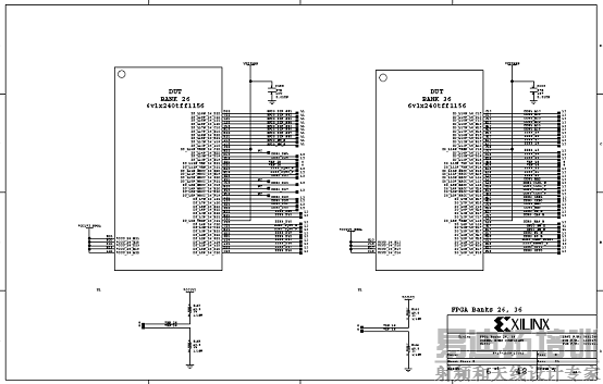
图11.ML605电路图(6)
图12.ML605电路图(7)
图13.ML605电路图(8)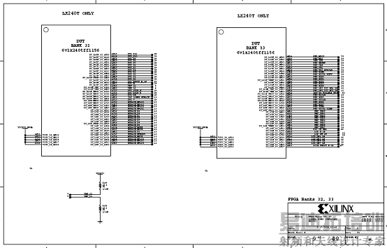
图14.ML605电路图(9)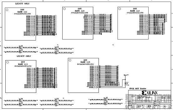
图15.ML605电路图(10)
射频工程师养成培训教程套装,助您快速成为一名优秀射频工程师...
天线设计工程师培训课程套装,资深专家授课,让天线设计不再难...
上一篇:基于CX25858设计的8路音视频译码方案
下一篇:利用低门限电压延长电池寿命技术
射频和天线工程师培训课程详情>>