- 易迪拓培训,专注于微波、射频、天线设计工程师的培养
ONSEMINCP125525W离线电流模式PWM控制器参考设计方案
The NCP1255 is a highly integrated PWM controller capable of delivering a rugged and high performance offline power supply in a SOIC
8 package. With a supply range up to 35 V, the controller hosts a jittered 65
kHz switching circuitry operated in peak current mode control. When the power on the secondary side starts to decrease, the controller automatically folds back its switching frequency down to a minimum level of 26 kHz. As the power further goes down, the part enters skip cycle while freezing the peak current setpoint.
To help build rugged converters, the controller features several key protective features: a brown
out, a non
dissipative Over Power Protection for a constant maximum output current regardless of the input voltage, two latched over voltage protection inputs – either through a dedicated pin or via the Vcc input
and finally, the possibility to externally adjust an auto
recovery timer duration.
The controller architecture is arranged to authorize a transient peak power excursion when the peak current hits the limit. At this point, the switching frequency is increased from 65 kHz to 130 kHz until the peak requirement disappears. The timer duration is then modulated as the converter crosses a peak power excursion mode (long) or undergoes a short circuit (short).
NCP1255主要特性:
65
kHz Fixed
frequency Current
mode Control Operation with 130
kHz Excursion
Internal and Adjustable Over Power Protection (OPP) Circuit
Adjustable Brown
Out Protection Circuit
Frequency Foldback down to 26 kHz and Skip
cycle in Light Load Conditions
Adjustable Slope Compensation
Internally Fixed 4
ms Soft
start
Adjustable Timer
based Auto
recovery Overload/Short
circuit Protection
100% to 25% Timer Reduction from Overload to Short
circuit Fault
Double Vcc Hiccup for a Reduced Average Power in Fault Mode
Frequency Jittering in Normal and Frequency Foldback Modes
Latched OVP Input for Improved Robustness and Latched OVP on Vcc
Up to 35
V Vcc Maximum Rating
Extremely Low No
load Standby Power
This is a Pb
Free Device
NCP1255应用:
Converters requiring peak
power capability such as printers power supplies, ac
dc adapters for game stations.
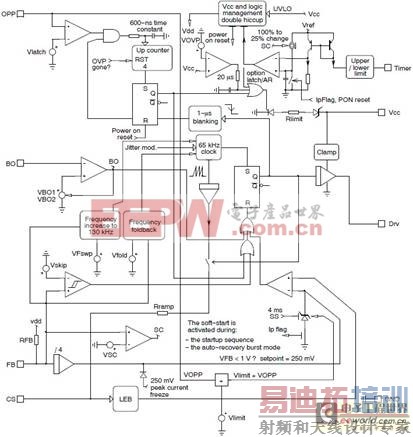
图1. NCP1255内部方框图
NCP1255方案介绍:
The NCP1255 features several novelties compared to the NCP1250 previously released. The key feature of this component lies in its ability to push the switching frequency as the converter experiences a sudden power increase.However, this available extra power delivery can only be maintained for a certain amount of time. Beyond this duration, the controller gives up and enters an auto-recovery mode. This mode is perfectly suited for converters supplying highly variable loads such as Haswell-based notebook adapters or inkjet printers to cite a few possible examples.
General Description
The part is encapsulated in a SOIC
8 package but a reduced-feature set version (no brown-out and timers are internally set), the NCP1254, also exists in a tiny TSOP
6 package. Featuring a low-power BiCMOS process, the die accepts to work with VCC levels up to 35 V, safely clamping the drive voltage below 12 V. With its 15 _A start-up current, a high-value resistive network can be used in offline applications to crank the converter, naturally minimizing the wasted power in high-line conditions. In nominal load operations, the switching frequency of this peak-current mode control circuit is 65 kHz.
When the power demand goes up, the controller increases the peak current setpoint until it reaches the upper limit (0.8 V over Rsense, no opp). At this point, the output power demand increase can only be answered by further shifting the switching frequency up until it reaches another limit, 130 kHz. The maximum power is thus obtained at this moment. On the contrary, in light-load operations, the part linearly reduces its switching frequency down to 26 kHz and enters skip cycle as power goes further down. This mode of operation favors higher efficiency from high to moderate output levels and ensures the lowest acoustic noise in the transformer. To improve the EMI signature, a low-frequency modulation brings some dither to the switching pattern. Unlike other circuits, the dither is kept in foldback and peak excursion modes, continuously smoothing the noise signature.
The part hosts several new protection means such as an auto-recovery brown-out circuit. It is adjustable via a resistive divider. A double hiccup on the VCC brings down the average input power while in auto-recovery fault mode.
Board Description
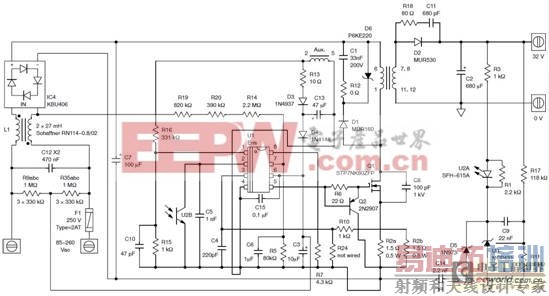
The application schematic that appears in Figure 1 has been optimized to limit the leakage inductance losses and maximize the efficiency. For this purpose, the RDC clamping network has been replaced by a TVS-based circuitry, leaving enough swing to the 800 V MOSFET. Again, a 600 V type could have been used but would have hampered the drain voltage dynamics at turn off. A capacitor in parallel with the TVS limits its peak current at the switch opening and helps softening the radiated noise. Besides its excellent performance in standby, the TVS approach helps to maintain a safe clamping level given the wide output power excursion.
The chip supply is brought in via pin 6. Please note that the start-up resistances, besides cranking the controller, also perform the X2 discharge function for free. Upon start-up, for a voltage less than 18 V (typical), the internal consumption is limited to 15 _A maximum. It suddenly changes to a few mA as the controller starts to drive the 800 V MOSFET at 130 kHz when VCC reaches 18 V. The auxiliary voltage can go down to around 9 V before the controller safely stops the switching pulses. The first VCC capacitor C3 must be sized so that the auxiliary winding takes over before the UVLO is touched. The auxiliary winding is tailored to deliver an auxiliary voltage above 12 V and it drops to 10 V in no-load conditions. This guarantees a good no-load standby power performance as you will read below. A low-valued resistance (R13) limits the voltage excursion on this auxiliary voltage in short circuit situations.
Regulation is ensured by pulling down the dedicated pin via an optocoupler, driven from the secondary side by a NCP431. This new device does not require a 1 mA bias current as it was the case with the classical TL431. The absence of this bias current greatly contributes to reducing the no-load standby power.
NCP1255方案原理图:
图2. NCP1255方案原理图
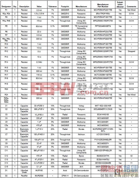
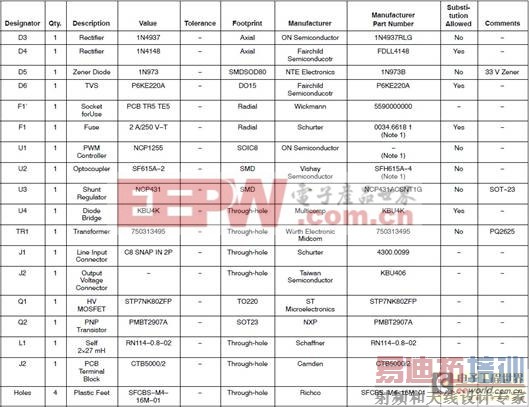
NCP1255方案材料清单:
PCB元件布局图:
射频工程师养成培训教程套装,助您快速成为一名优秀射频工程师...

