- 易迪拓培训,专注于微波、射频、天线设计工程师的培养
OnSemiNCV8855多输出电源控制解决方案
录入:edatop.com 点击:
On Semi公司的NCV8855是集成了高边负载开关的多输出电源控制器/稳压器,能满足汽车无线系统和仪表盘电源的要求. NCV8855还集成了开关电源(SMPS)降压控制器,2.5A SMPS降压稳压器和两个低压降(LDO)线性稳压器控制器,和超低静态电流的NCV861x一起能组成8输出的无线系统或仪表盘电源解决方案.器件满足ES
XW7T
1A278
AB测试脉冲G负载条件,VIN工作电压9.0V-18.0V.本文介绍了NCV8855主要特性, 应用电路/方框图, 汽车无线电系统框图以及NCV8855评估板电路图与材料清单.
The NCV8855 is a multiple output controller / regulator IC with an integrated high side load switch. The NCV8855 addresses automotive radio system and instrument cluster power supply requirements. In addition to the high side load switch, the NCV8855 includes a switch mode power supply (SMPS) buck controller, a 2.5 A SMPS buck regulator and two low dropout (LDO) linear regulator controllers. The NCV8855 in combination with the ultra low quiescent current NCV861x IC forms an eight output automotive radio or instrument cluster power solution. The NCV8855 has an internally set switching frequency of 170 kHz, with a SYNC pin for external frequency synchronization.
The NCV8855 is intended to supply power to various loads, such as a tuner, CD logic, audio processor and CD / tape control within a car radio. The high side switch can be used for a CD / tape mechanism or switching an electrically powered antenna or display unit. In an instrument cluster application, the NCV8855 can be used to power graphics display, flash memory and CAN transceivers. In addition, the high side switch can be used to limit power to a TFT display during a battery over voltage condition.
NCV8855主要特性:
1 uA Shutdown Current
Meets ES XW7T 1A278 AB Test Pulse G – Loaded Conditions
VIN Operating Range 9.0 to 18.0 V
1 SMPS Controller with Adjustable Current Limit
1 SMPS Regulator with Internal 300 m NMOS Switch
2 LDO Controllers with Current Limit and Short Circuit Protection
1 High side Load Switch with Internal 300 m NMOS FET
Adjustable Output Voltage for All Controllers / Regulators
800 mV, +/-1% Reference Voltage
System Enable Pin
Single Enable Pin for Both LDO Controllers
Independent Enable for High side Load Switch
Thermal Shutdown with Thermal Warning Indicator
This is a Pb Free Device
NCV8855应用:
Automotive Radio
Instrument Cluster, Driver Information System (DIS)
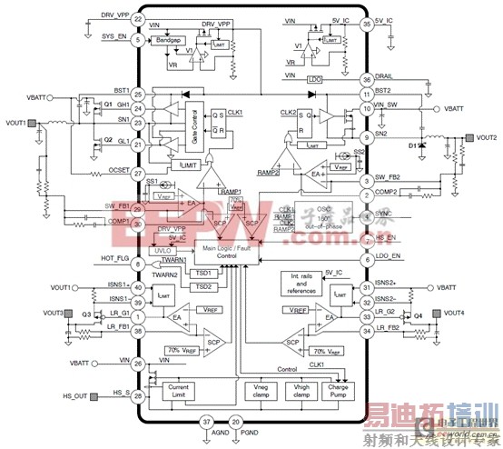
图1. NCV8855应用电路/方框图
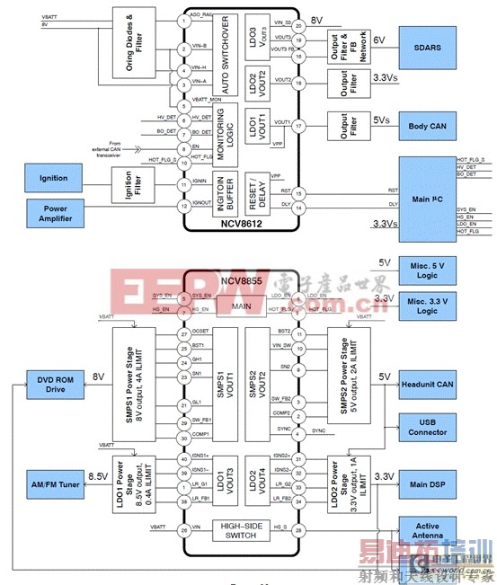
图2. NCV8855和NCV8612汽车无线电系统框图
NCV8855评估板
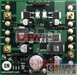
图3.评估板NCV8855BMNR2GEV外形图
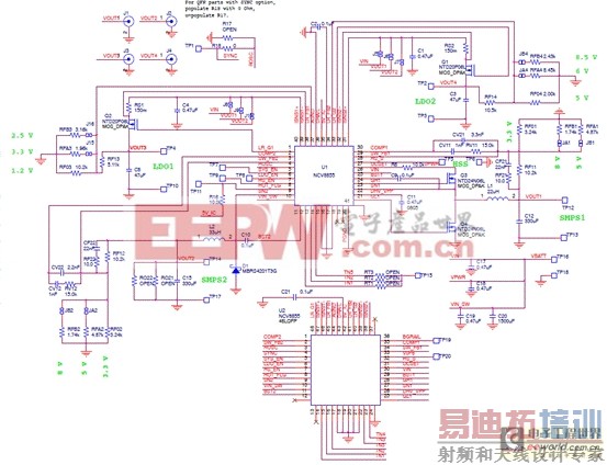
图4.评估板NCV8855BMNR2GEV电路图
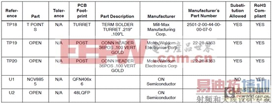
评估板NCV8855BMNR2GEV材料清单:


详情请见:
http://www.onsemi.cn/pub_link/Collateral/EVBUM2120-D.PDF
和
http://www.onsemi.cn/pub_link/Collateral/NCV8855BMNR2GEVB_SCHEMATIC.PDF
The NCV8855 is a multiple output controller / regulator IC with an integrated high side load switch. The NCV8855 addresses automotive radio system and instrument cluster power supply requirements. In addition to the high side load switch, the NCV8855 includes a switch mode power supply (SMPS) buck controller, a 2.5 A SMPS buck regulator and two low dropout (LDO) linear regulator controllers. The NCV8855 in combination with the ultra low quiescent current NCV861x IC forms an eight output automotive radio or instrument cluster power solution. The NCV8855 has an internally set switching frequency of 170 kHz, with a SYNC pin for external frequency synchronization.
The NCV8855 is intended to supply power to various loads, such as a tuner, CD logic, audio processor and CD / tape control within a car radio. The high side switch can be used for a CD / tape mechanism or switching an electrically powered antenna or display unit. In an instrument cluster application, the NCV8855 can be used to power graphics display, flash memory and CAN transceivers. In addition, the high side switch can be used to limit power to a TFT display during a battery over voltage condition.
NCV8855主要特性:
1 uA Shutdown Current
Meets ES XW7T 1A278 AB Test Pulse G – Loaded Conditions
VIN Operating Range 9.0 to 18.0 V
1 SMPS Controller with Adjustable Current Limit
1 SMPS Regulator with Internal 300 m NMOS Switch
2 LDO Controllers with Current Limit and Short Circuit Protection
1 High side Load Switch with Internal 300 m NMOS FET
Adjustable Output Voltage for All Controllers / Regulators
800 mV, +/-1% Reference Voltage
System Enable Pin
Single Enable Pin for Both LDO Controllers
Independent Enable for High side Load Switch
Thermal Shutdown with Thermal Warning Indicator
This is a Pb Free Device
NCV8855应用:
Automotive Radio
Instrument Cluster, Driver Information System (DIS)

图1. NCV8855应用电路/方框图

图2. NCV8855和NCV8612汽车无线电系统框图
NCV8855评估板

图3.评估板NCV8855BMNR2GEV外形图

图4.评估板NCV8855BMNR2GEV电路图
评估板NCV8855BMNR2GEV材料清单:


详情请见:
http://www.onsemi.cn/pub_link/Collateral/EVBUM2120-D.PDF
和
http://www.onsemi.cn/pub_link/Collateral/NCV8855BMNR2GEVB_SCHEMATIC.PDF
射频工程师养成培训教程套装,助您快速成为一名优秀射频工程师...
天线设计工程师培训课程套装,资深专家授课,让天线设计不再难...
上一篇:电力系统中的谐波问题及其解决方法
下一篇:电源技术中I2C及PM
Bus总线介绍
射频和天线工程师培训课程详情>>

