- 易迪拓培训,专注于微波、射频、天线设计工程师的培养
薄膜晶体管和超大规模集成电路:竞争与合作
Thin-Film Transistor and Ultra-Large Scale Integrated Circuit:
<
xml:namespace prefix = o ns = "urn:schemas-microsoft-com:office:office" />
Competition or Collaboration
Yue KUO
Thin Film Nano and Microelectronics Research Laboratory, <
xml:namespace prefix = st1 ns = "urn:schemas-microsoft-com:office:smarttags" />
Thin-film transistor (TFT) and ultra-large scale integrated circuit (ULSIC) have been compared and discussed with respect to the development history, technology trends, and applications. Detai
led
issues on materials, processes, and devices in the largearea TFT array fabrication and nano-size metal–oxide–s
emi
conductor field ef
fec
t transistors (MOSFETs) composed ULSIC on large wafers were also examined. The TFT fabrication processes were originally derived from ULSIC. However, there are many unique large-area processes and theories developed during the study of the TFT array fabrication, which
can
greatly benefit the future large wafer ULSIC production process. Although their future applications will be in different areas, there are opportunities that TFTs can be integrated into ULSIC products to enhance the functions and pe
rf
ormance.
[DOI: 10.1143/JJAP.47.1845]
KEYWORDS:
thin-film transistors, TFTs, ultra-large scale integrated circuits, ULSICs
1. Introduction
Thin film transistor (TFT) is a metal–insulator–semiconductor field-effect transistor (MISFET) device similar to the metal–oxide–semiconductor FET (MOSFET) used in the ultra large scale integrated circuit (ULSIC). The original MISFET concept was reported 1925.1) The ULSIC era started after the first report of the solid state bipolar transistor in 1947, but the industry grew dramatically after the introduction of the MOSFET device in 1960. Today, most of the ULSIC products are for high speed, high density logics or memories used in computers and related products. The first TFT was reported in 1962 but the TFT liquid crystal display ( LCD ) industry boosted after the disclosure of the first hydrogenated amorphous silicon (a-Si:H) TFT in 1979.2) The TFT application is focused on one type of product, i.e., active matrix (AM) LCDs, although TFTs can be used into many other types of products, e.g., light emitting diodes (LEDs), electroluminescences (ELs), organic LEDs ( OLED s), field-emission displays (FEDs), and electrophoretic displays.3)
Figure 1 shows state-of-the-art substrate sizes for the TFT glass and the ULSIC wafer as well as their basic transistor structures. Each glass is divided into several display back planes each of which is composed of millions of TFTs and related storage capacitors interconnected with two or three levels of metal lines. Each wafer is divided into hundreds or thousands of dies each of which is composed of millions of billions of MOSFETs and related devices interconnected with more than ten levels of metal lines. Substrate sizes of the two technologies are very different. Currently, the state-of- the-art wafer size is
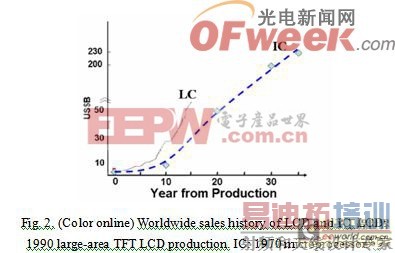
The IC industry blossomed with the introduction of complimentary MOSFETs ( CMOS FETs) to memories and microprocessors in early 1970s. The worldwide ULSIC business was about $230B in 2006. The commercial production of TFT LCDs started quickly since the report of the first functional a-Si:H TFT in 1979. The first mass production of large-area TFT LCDs started in 1990 and the worldwide sale reached over $50B in 2006.6,7) Figure 2 shows the market value vs. the production year of the two types of products. For IC, the count started from 1970 when microprocessors were mass produced.6) For LC, the count started when 10.4-in. TFT LCDs were mass produced in 1990.7) In spite of the very small product range of TFTs, i.e., LCDs only, and the large product range of ICs, for the first 15 years, the former’s growth rate is larger than the latter’s rate. However, in this period of time, TFT LCDs are exclusively used for computers or instruments, which are dependent on the availability of ULSIC chips. Therefore, the current success of the TFT business is to a great extent contributed by ULSIC products, specifically the periphery drivers.
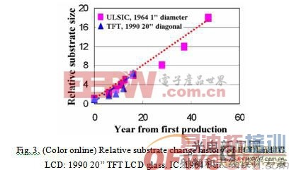
The substrate size directly influences the production throughput and therefore, the cost. Figure 3 shows changes of the relative substrate size of the TFT glass plate and the ULSIC wafer vs the production year. The rectangular glass with a diagonal size of about
TFT and ULSIC are silicon based mass production technologies. There are many efforts in preparing TFTs using non-silicon semiconductors. CdSe TFTs have been popular before 1980. Recently, organic and ZnO TFTs have made major progresses.9,10) The former has the potential of being fabricated without using the vacuum technology. The latter can be prepared by sputtering. These TFTs can be made into various chemical, photonic, and electrical sensors.11) Their low process temperature is also attractive for flexible displays. However, compared with a-Si:H and polycrystalline silicon (poly-Si) TFTs, they are in the development stage and need time to find proper markets.
<
xml:namespace prefix = v ns = "urn:schemas-microsoft-com:vml" />

Although a-Si:H and poly-Si TFTs have been successfully used as the pixel driving device in LCDs, it has been a long term goal for researchers to fabricate complicate circuits or novel products with this technology. The major advantage, which is also the biggest challenge, of the TFT technology
is its capability of achieving high performance devices on substrates with low glass transition temperatures, such as glass or plastics. Recently, there are some new developments in this area, for example:
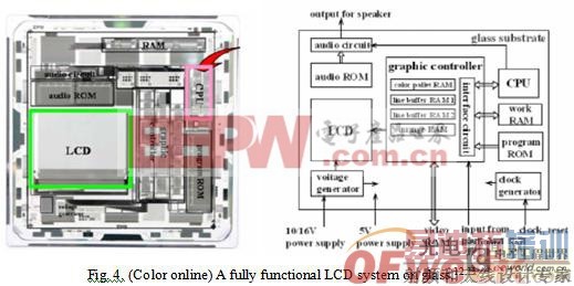
– Complete display system on glass. A complete LCD system, which includes a 2.2-in. LCD, central processing unit (CPU), read-only memory (ROM), random access memory (RAM), graphic controller, audio circuit, etc. on a 5-in. glass, has been demonstrated, as shown in Figs. 4(a) and 4(b).12,13) Circuits with 11 MHz operation frequency composed of n- and p-type poly-Si TFTs were fabricated by a solid phase crystallization method.13) This is a proof of the feasibility of fabricating of a multi-functional system on a commercial glass.
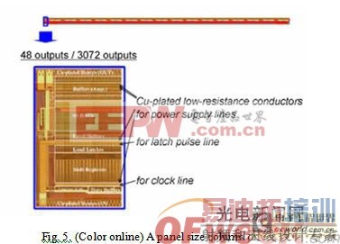
– Panel size drivers. Two types of panel size drivers have been fabricated based on poly-Si TFTs. The first type is the integrated driver which is fabricated during the construction of the back panel TFT array. This type of plate has been demonstrated with an additional ambient light sensor system constructed.13) The second type is the independent row or column driver, as shown in Fig. 5, which is fabricated separate from the back plate TFT array.14) This kind of driver can be used to drive existing a-Si:H or poly-Si TFT arrays. Each display requires only two pieces of drivers, i.e., one for gate and one for column. Therefore, one piece of the panel size driver can replace several pieces of IC driver chips. By integrating the peripheral driver ICs with the TFT fabrication process, the TFT business (at least poly-Si TFT LCDs) becomes more independent to the ULSIC because of no necessity of outsourcing the driver ICs.15)
– RFID s. High frequency, e.g., 13.56 MHz, and ultra high frequency, e.g., 1 GHz, RF circuits have been fabricated using poly-Si TFTs on flexible and solid substrates.16–18) These poly-Si TFTs were fabricated with different methods, e.g., continuous grain growth or m-Czochralski methods below 600 oC.16–18) These results enable the high performance RFIDs combined with flexible antennas.
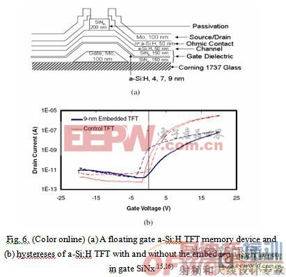
– Nonvolatile a-Si:H TFT memories. Flash memories made from poly-Si TFTs with ONO or floating-gate dielectric structures have been reported in the literature. 19–21) However, memories made from a-Si:H TFTs are rarely reported. Recently, the floating gate a-Si:H TFT has been fabricated into nonvolatile memories on a glass substrate at ≤ 300 oC, as shown in Fig. 6(a).22) It has a much larger hysteresis in transfer characteristics than the conventional a-Si:H TFT, as shown in Fig. 6(b).23) Memory capacitors based on the similar structure have also been demonstrated. 24) The ability of including low-temperature prepared memories to the logic circuit is desirable for both TFT circuits and ULSICs.
These recent developments raised the question on whether TFT and ULSIC will become competitive or complimentary technologies in the future.
2. Comparison of Devices, Materials, and Fabrication Processes
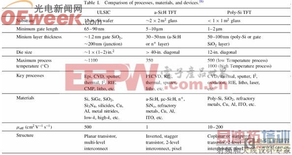
In order to compare TFT and ULSIC technologies, their basic material, process, and device properties need to be studied. Table I lists some important properties.25) These properties are closely related to product performance. For example, since the early development stage, the TFT application was focused on LCD pixel driving. The low temperature glass was the substrate of choice. Therefore, the fabrication process has to satisfy requirements of 1) largearea substrates, 2) low temperatures, and 3) high throughputs. Although most of the TFT fabrication processes were originated from ULSIC processes, there are many unique problems that cannot be solved directly from existing knowledge. New phenomena and theories have been developed during the developing of the large-area, lowtemperature TFT production process. Since some of the TFT material and process requirements are more stringent than those of the ULSIC, these new results can greatly benefit the future large wafer ULSIC process development. The following are some examples:
2.1 Large-area PECVD thin films
Plasma-enhanced chemical vapor deposition (PECVD) is the dominant thin film deposition method for a-Si:H, nt, and SiNx layers. The availability of the doped PECVD a-Si:H film is critical to the successful demonstration of the first a-Si:H TFT.26) During the large-area PECVD SiNx study, a generalized relationship that correlated the plasma power to deposition rate, uniformity, refractive index, stress, and plasma phase particle generation has been developed.27–29) TFT characteristics, e.g., threshold v olt age, are correlated to SiNx gate dielectric properties, e.g., refractive index.30) The PECVD a-Si:H deposition condition can affect the interface composition of the underneath SiNx gate dielectric through the hydrogen etching mechanism.31) The damaged interface has a large interface density of states, which lowers the threshold voltage and the field effect mobility. The hydrogen etching mechanism also plays an important role in the microcrystalline (mc) phase formation in mc-Si:H.32) The simultaneous deposition-and-etching mechanism in PECVD is critical to inter-layer dielectric, passivation, etc., which are common in ULSICs.
2.2 Plasma etching processes
Plasma etching in ULSIC is mainly used on low pressure CVD (LPCVD) or sputtered thin films with a preferred vertical profile. The most common etching damage is the charge neutralization caused breakdown of the thin gate dielectric. Plasma etching is also critical to the TFT array fabrication. Most of the etched thin films are deposited by PECVD, such as a-Si:H, SiNx, or nt, or sputtering, such as refractory metals. The former has a high hydrogen content, which corresponding to a high etch rate but low etch selectivity between two films. The plasma chemistry and the ion bombardment energy are both important to the etch process.33–35) Plasma etch induced damages in the a-Si:H TFT are mainly from the short wavelength light radiation, which can be repaired by a thermal annealing step.36) For the latter, when the gate line is etched, a sloped profile is necessary.37,38) These problems are rarely discussed in ULSICs. However, low thermal budget processes, such as PECVD, are important to nano-size MOSFET fabrication. In another case, the high-k gate dielectric contains noncovalent bonds that are subject to plasma radiation damages. Therefore, the TFT plasma etching results are potentially important to the future generation ULSIC fabrication.
2.3 Simplified fabrication processes
The dramatic ramp up the large-area TFT array production throughput is greatly contributed by the aggressive reduction of the number of masks, e.g., from 7 – 8 masks in early
2.4 Large-area laser processes
Laser crystallization is one of the most critical process steps in preparing high mobility, low threshold voltage, and low subthreshold slope poly-Si TFTs.42) Novel laser crystallization techniques, such as the metal-induced, lateral crystal growth, phase-modulated, or selective re-radiation method, have been used to prepare poly-Si thin films.43–46) Laser processes have been used in producing poly-Si TFTs on large-area glass substrates. For advanced ULSIC fabrication, laser has been used in preparing submicron structures, such as filling the small vias with the deposited Al or Cu film, shallow junction doping, activation of implanted dopants, and formation of a thin gate oxide layer.47–49) However, laser processing is rarely used in mass production of ULSICs probably due to the concern of large-area issues. Therefore, the TFT experience in laser processing may be a great help to the ULSIC production especially on large size wafers.
2.5 High-k gate dielectrics
Since the early development of the large-area a-Si:H TFT array fabrication, high-k dielectrics, such as SiNx, Ta2O5, HfO2, or Al2O3, have been used as the gate dielectric material.50–53) Due to its high k value, a phy sically relative thick film can be used to avoid the shortage between the top (source/drain) and bottom (gate) metals as well as to reduce the gate current leakage. However, in order to achieve the best device characteristics, such as high field effect mobility, low interface density of states, and the low threshold voltage, the high-k material is used as the bulk gate dielectric film with a separate SiNx interface layer in contact with a-Si:H.54,55) The interface SiNx layer usually contains nonstoichiometric composition, smooth interface, low stress, low defect density, etc.30,56,57) For sub 65 nm MOSFETs, a high-k material is required to replace the sub 1.2 nm thick thermal SiO2 gate dielectric to reduce the leakage current, to eliminate the diffusion of dopants to the channel region, and to improve device reliability.58) However, when the metal oxide high-k film is in direct contact with the silicon substrate, under a high temperature thermal annealing condition, it forms a defective SiOx or silicate interface layer that lowers the effective dielectric constant and generates a high interface state density.59–62) This problem could be solved by inserting an artificial interface layer of SiO2 or SiON.63,64) This result is consistent with that of TFT. Furthermore, for nano-size devices, the interface structure and properties are sensitive to the fabrication process condition. There is a general trend of preparing the ultrathin film under the non-equilibrium thermodynamic condition, such as the flash or pulsed thermal annealing, plasma exposures, or graded thin films. For example, our recent result showed that the sub 1 nm equivalent oxide thickness (EOT) high-k stack was achieved with a proper interface layer structure prepared under a tight annealing condition.65) Since most a-Si:H TFT processes are done at low temperatures and under thermodynamically non-equilibrium conditions, the experience would be useful for the nano-size device fabrication on large-size wafers.
2.6 Transistor structures
The structure of a transistor influences the device performance, product rel [p] iability, and production throughput. For example, for the a-Si:H TFT, the inverted staggered structure gives better mobility, threshold voltage and current on/off ration. For the poly-Si TFT, the conventional coplanar structure shows a high leakage current and serious kink and hot carrier effects. Although grain boundary hydrogenation can be used to solve the problem, a lte red transistor structures, such as the multiple gate, offset gate, field-induced drain, double gate, buried channel, or vertical channel, are also effective.66) Many of these new structures also showed improved transistor characteristics, such as a large on current, due to the increased channel width/length ratio. Recently, the aggressive shrinking of the channel length of the MOSFET imposes a great challenge to the lithography area. While it takes a long time to develop the manufacturable sub 50 nm lithography equipment and process, new transistor structures, such as the FinFET and dual gate, have also been proposed.67,68) Some of the MESFET structures are similar to the above poly-Si structures.
Previously, it was discussed that the throughput of the TFT production could be increased by reducing process steps, such as using new transistor structures. For example, the a-Si:H TFT can be fabricated with only two masks.40) In another case, the complete a-Si:H TFT array with the storage capacitor could be fabricated with 4 – 5 masks.39) Even the complete CMOSFETs can be fabricated with five masking steps.41) Therefore, TFT and ULSIC experiences in using new transistor structures to improve device performance or production throughput can benefit each other.
3. Future Applications and Collaborations
Since MOSFETs approaching the nano size, the ULSIC chip will eventually contain giga number of transistors operated in the tera-hertz frequency. This is achievable due to the near-perfect single crystal wafer substrate as well as years of advancements in fabrication processes and understanding of device physics. Although the single electron device has been demonstrated,69,70) the physical limitation of the MOSFET size, e.g., the channel length, has not been determined. Additionally, there are constant efforts in creating optical devices based on the silicon technology. The recent demonstration of light emission from the nanocrystalline silicon
embedded
SiO2 71,72) expanded ULSIC to optical memories and possible interconnects.
The major advantage of the a-Si:H TFT is its low process temperature, which removes many limits on the substrate material and size. Its structures and composing materials are easy to alter to satisfy application needs. The a-Si:H TFT can be connected to many organic or inorganic materials or devices. The product’s sensing function may be further enhanced with the low- or high-speed TFT circuit, which is an unexplored area with much potential. Separately, the lowtemperature a-Si:H TFT nonvolatile memories have been demonstrated.24) Therefore, in spite of its low mobility, the a-Si:H TFT can be used to drive or to operate as a chemical, electrical, biological, and optical sensor.11,73–81)
Although the field effect mobility of the individual poly-Si TFT can be as high as or even higher than that of a MOSFET,82) the current poly-TFT circuit speed is usually slower than that of the ULSIC, e.g., GHz vs >GHz.14) However, the former is fabricated on the low-cost glass substrate at a medium temperature, e.g., 550 oC, which has advantages of the low production cost and the large product size. In principle, the poly-Si TFT circuit can be fabricated on a flexible substrate using a low-temperature process. The poly-Si TFT is especially useful in driving devices that require a large current, such as the organic LED.83) Poly-Si TFT characteristics are often controlled by the bulk grain quality and grain boundary defect states. Since it is difficult to control the number and location of grain boundaries in the channel region in a large-area array, the reliability of the nano-size poly-Si TFT is a major concern. There are several methods being proposed to selectively forming the channel region within the single large grain,84–86) which are potential solutions for the problem. However, in addition to further improve the grain quality, the transistor structure, channel location, and circuit layout need to be optimized87) before the poly-Si TFT circuit can compete with the ULSIC in speed.
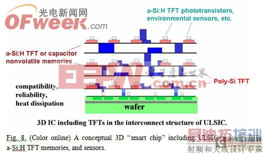
Although TFT and ULSIC applications are expected to expand in different areas, there are overlapped areas, as shown in Fig. 7. Different technologies may be integrated into the same product. An example is the three-dimensional (3D) ‘‘smart chip’’ design, as shown in Fig. 8. The front end process of the ULSIC can be fabricated with the conventional process. Then, the high-speed poly-Si TFTs can be constructed above it using the high-temperature or laser crystallization process. Subsequently, the slower poly-Si TFTs can be fabricated away from the wafer with a lowtemperature process, such as, the metal-induced crystallization. Furthermore, the floating gate a-Si:H TFT nonvolatile memories can then be constructed near the top layer of the interconnect structure at a temperature lower then the typical interconnect process temperature. Finally, a-Si:H based sensors can be added on top of the chip to detect changes of light, hu mid ity, etc. Signals of environmental changes can be fed to the 3D circuit to adjust it functions, e.g., speed, memory, or energy consumption. The a-Si:H pin diode has been fabricated on top of an ASIC as the photo sensor.88) However, the split-gate a-Si:H TFT can also be used as a photo sensor, which does not require the low dopant efficiency pt thin film deposition step.75) In addition, special materials or structures of the a-Si:H TFT can be used to detect other environmental parameters, such as the pH value in a solution or the components in a gas stream. Since the source, drain, and gate electrodes of all these TFTs can be made of the same interconnect metal of the ULSIC, only a couple of extra masks are required to complete the TFT. In principle, this kind of conceptual chip can be constructed with the current process technology. However, for the actual operation, issues, such as process compatibility, reliability, and heat dissipation, need to be investigated in detail.

4. Summary
TFT and ULSIC are originated from the same concept. They both have been developed into gigantic industries with separate markets. Originally, TFT fabrication processes were derived from ULSIC processes. However, due to its unique temperature and substrate requirements, new knowledge on process chemistry and physics has been obtained, which is potentially important for the production of future nanodimension MOSFETs in large-size wafers. In this paper, the author compared and discussed the a-Si:H TFT, poly-Si TFT, and ULSIC technologies with respect to materials, processes, and devices. In the long term, their main applications will be in different fields due to different strengths and restrictions. However, in certain areas, these technologies may be integrated into one product such as the 3D ‘‘smart chip’’.
Acknowledgement
The author would like to acknowledge his graduate students and postdoctoral scholars for their dedicated work in both TFT and ULSIC areas. He also thanks financial supports from various funding agencies, such as NSF, other government agencies, and industry companies. The author also acknowledges the precious hands-on experience he gained from near two decades of industry service in
1) R. G. Arns:
2) Y. Kuo: ECS Trans. 6 (2007) No. 4, 121.
3) Y. Kuo: in Amorphous Silicon Thin Film Transistors, ed. Y. Kuo (Kluwer,
4) T. Tsukada:
IEEE
Trans. Electron Devices 38 (1991) 2689.
5) IRTS Factory Integration TWG, ‘‘
6) Economics Report, IC knowledge, Chap. 2 (http://www.icknowledge. com/our_products/Chapter PERCENT_202.pdf).
7) Y. Ishii: AM-
FPD
06 Dig. Tech. Pap. 2006, p. 1.
8) Y. Kuo: in Amorphous Silicon Thin Film Transistors, ed. Y. Kuo (Kluwer,
9) C. D. Dimitrakopoulos and D. J. Mascaro: IBM J. Res. Dev. 45 (2001) 11.
10) P. F. Carcia, R. S. McLean, M. H. Reilly, and G. Nunes, Jr.: Appl. Phys. Lett. 82 (2003) 1117.
11) Y. Kuo: AM-FPD 06 Dig. Tech. Pap., 2006, p. 77.
12) T. Ikeda, Y. Shionoiri, T. Atsumi, A. Ishikawa, H. Miyake, Y. Kurokawa, K. Kato, J. Koyama, S. Yamazaki, K. Miyata, T. Matsuo, T. Nagai, Y. Hirayama, Y. Kubota, T. Muramatsu, and M. Katayama: SID Int. Symp. Dig. Tech. Pap. 35 (2004) 860.
13) Y. Yamomoto and A. T. Voutsas: ECS Trans. 3 (2006) No. 8, 11.
14) H. Hayama: ECS Trans. 3 (2006) No. 8, 3.
15) S. Uchikoga and
16) T. Takayama, Y. Ohno, Y. Goto, A.
Mac
hida, M. Fujita, J. Maruyama, K. Kato, J. Koyama, and S. Yamazaki: VLSI Technology Dig. Tech. Pap., 2004, p. 230.
17) J. Koyama, Y. Kurokawaa, T. Ikeda, M. Endo, H. Dembo, D. Kawae, T. Inoue, M. Kozuma, D. Ohgarane, S. Saito, K. Dairiki, H. Takahashi, and S. Yamazaki: ECS Trans. 8 (2007) No. 1, 57.
18) N. Saputra, M. Danesh, A. Baiano, R. Ishihara, J. R. Long, J. W. Metselaar, C. I. M. Beenakker, N. Karaki, Y. Hiroshima, and S. Inoue: Proc. European Solid-State Device Research Conf. (ESSDERC), 2007, C
19) S.-I. Hsieh, H.-T. Chen, Y.-C. Chen, C.-L. Chen, and Y.-C. King: IEEE Electron Device Lett. 27 (2006) 272.
20) S. Shukuri, T. Kuri, T. Kobashi, Y. Gotoh, and T. Nishida: IEEE Trans. Electron Devices 41 (1994) 926.
21) K. Yano, T. Ishii, T. Hashimoto, T. Kobayashi, F. Murai, and K. Seki: IEEE Trans. Electron Devices 41 (1994) 1628.
22) Y. Kuo and H. Nominanda: Appl. Phys. Lett. 89 (2006) 173503.
23) Y. Kuo and H. Nominanda: Mater. Res.
Soc
. Symp. Proc. 989 (2007) A10-03.
24) H. Nominanda and Y. Kuo: Electrochem. Solid-State Lett. 10 (2007) H232.
25) Y. Kuo: ECS Trans. 8 (2007) No. 1, 45.
26) W. E. Spear and P. G. LeComber: Philos. Mag. B 33 (1976) 935.
27) Y. Kuo: Mater. Res. Soc. Symp. Proc. 282 (1992) 623.
28) Y. Kuo: Appl. Phys. Lett. 63 (1993) 144.
29) Y. Kuo: J. Electrochem. Soc. 142 (1995) 2486.
30) Y. Kuo: J. Electrochem. Soc. 142 (1995) 186.
31) Y. Kuo: Vacuum 59 (2000) 484.
32) Y. Kuo: Appl. Phys. Lett. 71 (1997) 2821.
33) Y. Kuo and M. Crowder: J. Electrochem. Soc. 139 (1992) 548.
34) Y. Kuo: J. Vac. Sci. Technol. A 8 (1990) 1702.
35) Y. Kuo: IBM J. Res. Dev. 36 (1992) 69.
36) Y. Kuo: Appl. Phys. Lett. 61 (1992) 2790.
37) Y. Kuo and J. R. Crowe: J. Vac. Sci. Technol. A 8 (1990) 1529.
38) Y. Kuo: J. Electrochem. Soc. 137 (1990) 1907.
39) C.-H. Oh, H.-C. Choi, and C.-H. Hong: Electrochem. Soc. Proc. 2002- 23 (2002) 1.
40) Y. Kuo: J. Electrochem. Soc. 138 (1991) 637.
41) H. Onishi, K. Imai, H. Nakamura, Y. Matsubara, Y. Yamada, T. Tamura, T. Sakai, and T. Horiuchi: VLSI Technology Dig. Tech. Pap., 1997, p. 33.
42) T. Sameshima: in Polycrystalline Silicon Thin Film Transistors, ed. Y. Kuo (Kluwer,
43) A. Imaya: AM-FPD 03 Dig. Tech. Pap., 2003, p. 104.
44) N. Sasaki: Electrochem. Soc. Proc. 2004-15 (2004) 1.
45) Y. Taniguchi, M. Matsumura, M. Jyumonji, H. Ogawa, and M. Hiramatsu: Electrochem. Soc. Proc. 2004-15 (2004) 18.
46) M. Hatano, H. Hamamura, M. Matsumura, Y. Toyota, M. Tai, M. Ohkura, and T. Miyazawa: ECS Trans. 3 (2006) No. 8, 35.
47) V. Surganov, A. Mozalev, and V. Boksha: Microelectron.
48) P. G. Carey, K. H. Weiner, and T. W. Sigmon: IEEE Trans. Electron Devices 35 (1988) 2429.
49) K. K. Ong, K. L. Pey, P. S. Lee, A. T. S. Wee, X. C. Wang, and Y. F. Chong: Appl. Phys. Lett. 89 (2006) 082101.
50) P. G. LeComber, W. E. Spear, and A. Ghaith: Electron. Lett. 15 (1979) 179.
51) E. Lueder: SID Int. Symp. Dig. Tech. Pap., 1980, p. 118.
52) F. Luo and O. Hoesly: SID Int. Symp. Dig. Tech. Pap., 1983, p. 46.
53) F. Funada, Y. Takafuji, K. Yano, H. Take, and M. Matsura: SID Int. Symp. Dig. Tech. Pap., 1986, p. 293.
54) M. Yoshida, T. Nomoto, Y. Sekido,
55) Y. Kuo: in Amorphous Silicon Thin Film Transistors, ed. Y. Kuo (Kluwer,
56) K. Hiranaka, T. Yoshimura, and T. Yamaguchi: J. Appl. Phys. 62 (1987) 2129.
57) H. Uchida, T. Takechi, S. Nishida, and S. Kaneko: Jpn. J. Appl. Phys. 30 (1991) 3691.
58) ITRS, 2001-2003 edition, SIA (http://public.itrs.net).
59) Y. Kuo: ECS Trans. 2 (2006) No. 1, 13.
60) Y. Kuo: ECS Trans. 3 (2006) No. 3, 253.
61) J.-Y. Tewg, Y. Kuo, J. Lu, and B. Schueler: J. Electrochem. Soc. 151 (2004) F59.
62) J. Lu, Y. Kuo, and J.-Y. Tewg: J. Electrochem. Soc. 153 (2006) G410.
63) J. F. Kang, H. Y. Yu, C. Ren, M.-F. Li, D. S. H. Chan, X. Y. Liu, and D.-L. Kwong: Electrochem. Solid-State Lett. 8 (2005) G311.
64) J. J. Peterson, C. D. Young, J. Barnett, S. Gopalan, J. Gutt, C.-H. Lee, H.-J. Li, T.-H. Hou, Y. Kim, C. Lim, N. Chaudhary, N. Moumen, B.-H. Lee, G. Bersuker, G. A. Brown, P. M. Zeitzoff, M. I. Gardner, R. W. Murto, and H. R. Huff: Electrochem. Solid-State Lett. 7 (2004) G164.
65) J. Yan, Y. Kuo, and J. Lu: Electrochem. Solid-State Lett. 10 (2007) H119.
66) R. Ishihara: in Polycrystalline Silicon Thin Film Transistors, ed. Y. Kuo (Kluwer,
67) D. Hisamoto, W.-C. Lee, J. Kedzierski,
68) X. Huang, W.-C. Lee, C. Kuo, D. Hisamoto, L. Chang, J. Kedzierski, E. Anderson, H. Takeuchi, Y.-K. Choi, K. Asano, V. Subramanian, T.-J. King, J. Bokor, and C. Hu: IEEE Trans. Electron Devices 48 (2001) 880.
69) K. Yano, T. Ishii, T. Hashimoto, T. Kobayashi, F. Murai, and K. Seki: IEEE Trans. Electron Devices 41 (1994) 1628.
射频工程师养成培训教程套装,助您快速成为一名优秀射频工程师...

