- 易迪拓培训,专注于微波、射频、天线设计工程师的培养
基于TOP265EG设计的30W待机电源方案
录入:edatop.com 点击:
TOPSwitch-JX系列(TOP264-271)集成了725V功率MOSFET,高压开关电流源,多模式PWM控制,热关断电路,故障保护和其它控制电路, 265 VAC电压下无负载的功耗低于100mW.本文介绍了TOPSwitch-JX系列(TOP264-271)主要特性, 方框图, 通用输入高效19V 65W反激电源电路图和采用TOP265EG的12V 30W高效待机电源设计案例的电路图和所用材料清单.
TOPSwitch-JX TOP264-271 cost effectively incorporates a 725 V power MOSFET, high voltage switched current source, multi-mode PWM control, oscillator, thermal shutdown circuit, fault protection and other control circuitry onto a monolithic device.
TOPSwitch-JX 系列主要特性:
EcoSmart® - Energy Efficient
Energy efficient over entire load range
No-load consumption below 100 mW at 265 VAC
Up to 750 mW standby output power for 1 W input at 230 VAC
High Design Flexibility for Low System Cost
Multi-mode PWM control maximizes efficiency at all loads
132 kHz operation reduces transformer and power supply size
66 kHz option for highest efficiency requirements
Accurate programmable current limit
Optimized line feed-forward for line ripple rejection
Frequency jittering reduces EMI filter cost
Fully integrated soft-start for minimum startup stress
725 V rated MOSFET
Simplifies meeting design derating requirements
Extensive Protection Features
Auto-restart limits power delivery to 3% during overload faults
Output short-circuit protection (SCP)
Output over-current protection (OCP)
Output overload protection (OPP)
Output overvoltage protection (OVP)
User programmable for hysteretic/latching shutdown
Simple fast AC reset
Primary or secondary sensed
Line undervoltage (UV) detection prevents turn-off glitches
Line overvoltage (OV) shutdown extends line surge withstand
Accurate thermal shutdown with large hysteresis (OTP)
Heat transfer to both PCB and heat sink
Optional external heat sink provides thermal impedance equivalent to a TO-220
eSIP®-7C package:
Vertical orientation for minimum PCB footprint
Simple heat sink mounting using clip provides thermal impedance equivalent to a TO-220
Extended creepage to DRAIN pin
Heat sink is connected to SOURCE for low EMI
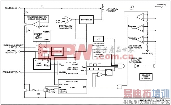
图1.TOPSwitch-JX系列功能方框图(E 和V 封装).
 [p]
[p]
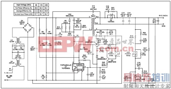
图2.TOPSwitch-JX系列通用输入高效19V 65W反激电源电路图
采用TOPSwitch-JX系列TOP265EG的12V 30W高效待机电源设计案例
12V 30W设计案例主要特性:
Highly energy efficient
Full load efficiency >90%
Efficiency >87% above 10% load
Average efficiency >90% (25%, 50%, 75%, 100% load points)
No-load input power 100 mW
Simplifies meeting ENERGY STAR 2.0, 80 Plus and EuP requirements
725 V MOSFET rating allowed high turns ratio (VOR) and use of 60 V Schottky output diode
Low cost, low component count and small PCB footprint solution
Performance met without synchronous output rectification
132 kHz operation optimized core size and efficiency performance
Low-profile eSIP package
Integrated Protection and Reliability Features
Line under-voltage lock out (UVLO)
Primary sensed latching output overvoltage shutdown (OVP) with fast AC reset
Auto recovery output over current (OCP)
Meets limited power source (LPS) 100 VA requirement with a single point of failure
Accurate thermal shutdown with large hysteresis
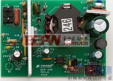
图3.设计案例PCB外形图(2.97 x 2.14 ).
设计电源指标:
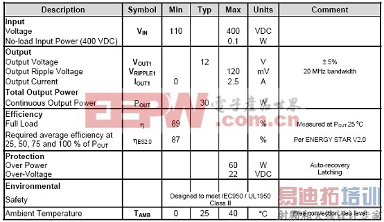
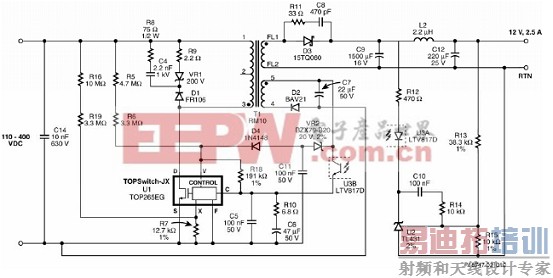
图4. 12V 30W设计案例电路图
设计案例材料清单:
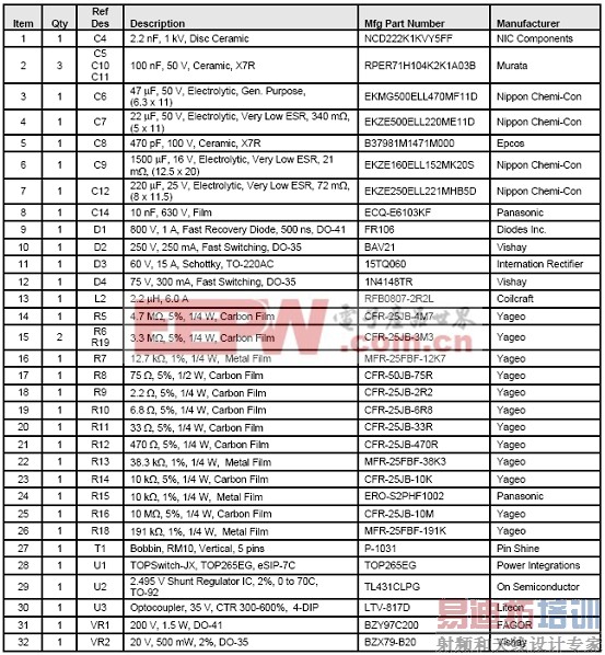

图5. 12V 30W设计案例变压器电框图
TOPSwitch-JX TOP264-271 cost effectively incorporates a 725 V power MOSFET, high voltage switched current source, multi-mode PWM control, oscillator, thermal shutdown circuit, fault protection and other control circuitry onto a monolithic device.
TOPSwitch-JX 系列主要特性:
EcoSmart® - Energy Efficient
Energy efficient over entire load range
No-load consumption below 100 mW at 265 VAC
Up to 750 mW standby output power for 1 W input at 230 VAC
High Design Flexibility for Low System Cost
Multi-mode PWM control maximizes efficiency at all loads
132 kHz operation reduces transformer and power supply size
66 kHz option for highest efficiency requirements
Accurate programmable current limit
Optimized line feed-forward for line ripple rejection
Frequency jittering reduces EMI filter cost
Fully integrated soft-start for minimum startup stress
725 V rated MOSFET
Simplifies meeting design derating requirements
Extensive Protection Features
Auto-restart limits power delivery to 3% during overload faults
Output short-circuit protection (SCP)
Output over-current protection (OCP)
Output overload protection (OPP)
Output overvoltage protection (OVP)
User programmable for hysteretic/latching shutdown
Simple fast AC reset
Primary or secondary sensed
Line undervoltage (UV) detection prevents turn-off glitches
Line overvoltage (OV) shutdown extends line surge withstand
Accurate thermal shutdown with large hysteresis (OTP)
Heat transfer to both PCB and heat sink
Optional external heat sink provides thermal impedance equivalent to a TO-220
eSIP®-7C package:
Vertical orientation for minimum PCB footprint
Simple heat sink mounting using clip provides thermal impedance equivalent to a TO-220
Extended creepage to DRAIN pin
Heat sink is connected to SOURCE for low EMI

图1.TOPSwitch-JX系列功能方框图(E 和V 封装).
 [p]
[p]
图2.TOPSwitch-JX系列通用输入高效19V 65W反激电源电路图
采用TOPSwitch-JX系列TOP265EG的12V 30W高效待机电源设计案例
12V 30W设计案例主要特性:
Highly energy efficient
Full load efficiency >90%
Efficiency >87% above 10% load
Average efficiency >90% (25%, 50%, 75%, 100% load points)
No-load input power 100 mW
Simplifies meeting ENERGY STAR 2.0, 80 Plus and EuP requirements
725 V MOSFET rating allowed high turns ratio (VOR) and use of 60 V Schottky output diode
Low cost, low component count and small PCB footprint solution
Performance met without synchronous output rectification
132 kHz operation optimized core size and efficiency performance
Low-profile eSIP package
Integrated Protection and Reliability Features
Line under-voltage lock out (UVLO)
Primary sensed latching output overvoltage shutdown (OVP) with fast AC reset
Auto recovery output over current (OCP)
Meets limited power source (LPS) 100 VA requirement with a single point of failure
Accurate thermal shutdown with large hysteresis

图3.设计案例PCB外形图(2.97 x 2.14 ).
设计电源指标:


图4. 12V 30W设计案例电路图
设计案例材料清单:


图5. 12V 30W设计案例变压器电框图
射频工程师养成培训教程套装,助您快速成为一名优秀射频工程师...
天线设计工程师培训课程套装,资深专家授课,让天线设计不再难...
上一篇:电流馈电推挽式逆变电路
下一篇:开关电源中X电容和Y电容设计规则
射频和天线工程师培训课程详情>>

