- 易迪拓培训,专注于微波、射频、天线设计工程师的培养
手机电源管理需要专门的IC
录入:edatop.com 点击:
By Jeff Falin, Texas Instruments
Introduction
Third generation "smart" cell phones combine the traditional 2G cellular phone with PDA-like features as well as digital still cameras (DSCs) and music players (MP3s). Figure 1 shows a simplified block diagram of a 3G phone with its major subsystems and their respective voltage rails.
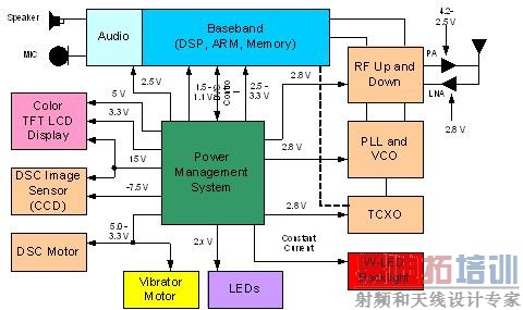
Figure 1 " 3G Smart
Such diversity in functionality requires numerous components, most of which have different power rail voltages, with each rail having growing power demands and application-specific requirements. At the same time, consumers want smaller phones with maximum battery life and minimal battery charge time. All of these requirements have driven development of various high performance and/or highly specialized power management integrated circuits (ICs). This article discusses how power management ICs have evolved to meet many of the requirements of the new smart phones.
The Battery
The input power source strongly influences power IC design. At present and into the near future, the Li-Ion rechargeable battery will be the power source for portable electronics. Its high volumetric and gravimetric energy densities (270-300 Wh/l and 110-130 Wh/kg, respectively) mean it provides more power for its size and weight than other battery types. Second, its 2.7 V to 4.2 V operating voltage is higher than the primary high current power rails. This means that high DC/DC conversion efficiencies, and therefore long battery life, are possible because stepping down (or bucking) a higher voltage rail to a lower voltage rail is almost always more efficient than stepping up (or boosting) to a higher voltage rail.
Proper management and control of a rechargeable battery is critical for maximizing battery life. Battery management consists of three parts: battery monitoring, battery protection and charge control. Battery monitoring and protection ICs are typically packaged with the battery itself. However, charge control is part of the portable device. Charge control ICs have evolved significantly from simple linear controllers with only basic protection and control circuitry to switching DC/DC converters with integrated switches and features to meet user demands, such as reduced charge time. Early linear charger ICs had lower efficiency, computed as output voltage over input voltage, and therefore either their input voltage or their charging current was limited by the power dissipation capabilities of the package.
Recently, semiconductor manufacturers have been developing not only processes with lower minimum gate lengths for higher-density and higher-speed digital circuitry, but also drain-extended devices capable of higher voltages for more analog and power applications. TI's bq24100 switch-mode battery charging IC with internal power FETs, for example, has the digital circuitry to provide the protection and control required of a battery charger. Its wide input voltage range, up to 16 V, makes it useful for charging one to three Li-Ion cells in series. It is capable of supplying up to 2 A of charge current for fast battery charging. Although it is packaged in a small 3.5 mm x 4.5 mm QFN package, power dissipation concerns are minimized due to its highly efficient PWM switching converter, which has peak efficiency above 92 percent.
Falling voltage rails with "tighter" tolerances
As demands increase for improved IC functionality at lower operating voltages and smaller packages, there are more stringent tolerance and efficiency requirements on the power management blocks. For example, imposing ±3 percent tolerance on a 1.2-V DSP power rail requires that the output not vary more than ±36mv versus a 3.3-V I/O rail with a ±3 percent tolerance being allowed ±99 mV of variance. Load transient responses on the order of 50 mV to 100 mV are not uncommon from traditional buck converters with 2% dc voltage tolerance and 100-uF output capacitance, preventing them from meeting the ± 3 percent tolerance, including load transients, without additional capacitors.
Newly developed IC fabrication processes have lower leakage currents and lower resistances (sometimes through copper overlay). This translates into FETs with lower quiescent currents and lower on-resistances, respectively. At the same time, shrinking technology nodes produce smaller FETs, which allow for smaller overall die and package size, lower operating voltages, and lower gate capacitances, all of which result in faster switching speeds. These advances have resulted in converters with tighter tolerances and extremely high efficiency in tiny packages.
This is exemplified in TI's new TPS62300, 500-mA DC/DC step-down converter with integrated FETs in a 2 mm x 1 mm chip scale package. Switching at 3-Mhz allows the converter to use small inductors in the 1 uH range, which can be found in an 0805 package, resulting in a total power solution (including input and output capacitors) of 5 mm x 5 mm. As an added benefit, the increase in switching frequency also allows for an increase in bandwidth of the control loop, thus improving switched load response. As a rule of design, the cross over frequency of the control loop is usually set to one sixth to one tenth of the switching frequency in order to maintain stability. Using a 500-KHz switcher with a cross over of one tenth the switch frequency gives a usable bandwidth of 50 KHz.
Increasing the frequency to 3 MHz would increase the bandwidth to 300 KHz which greatly improves the dynamic response of the power supply and thus makes designing tight tolerance power supplies achievable. Specifically, the IC can deliver DC voltage regulation accuracy from -0.5 to 1.3 percent over the entire industrial temperature and load current range. In addition, the control loop allows the use of low value, low ESR ceramic output capacitors without sacrificing transient response. As shown in Figure 2, with only 10 μF of low ESR ceramic output capacitance, the TPS6230x family of ICs has less than 25 mV droop during a 10 mA to 400 mA load transient. Additional output capacitance will further reduce the droop.
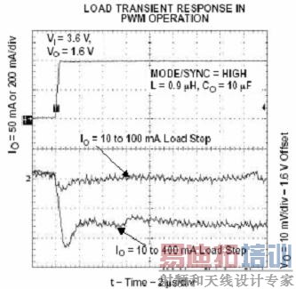
Figure 2 "Load transient response.
Dynamic or adaptive voltage scaling
Two of the most power hungry components in a smart phone are the baseband processor (DSP and ARM) and the RF power amplifier (PA). The power dissipated in a digital processor is directly proportional to the square of the voltage. When in standby or some other reduced functionality mode where the processor can operate at a lower frequency, the voltage can be reduced in order to lower power dissipation and achieve higher efficiency and longer battery life. Similarly, a PA is optimized to have highest efficiency at maximum transmit power. Since most cell phones operate relatively close to a base-station, the phone reduces transmit power to the minimum needed to maintain quality communication. At the reduced power levels, the PA efficiency suffers unless its power rail voltage is adjusted. Dynamic or adaptive voltage scaling links the processor or PA and the DC/DC converter providing its power rail in a feedback loop that dynamically adjusts the power supply voltage to the minimum level needed for proper operation.
With traditional power converter IC, the stability and switching characteristics are highly dependant on the input and output voltage values. This makes it difficult to design a stable, variable output voltage supply. The TPS6230x family of converters use a control method based on constant loop gain. A voltage is applied to the ADJUST (ADJ) pin of the TPS6230x to set the output voltage. The converter multiplies the voltage at the ADJ pin by a 1.5 to determine the output voltage. Since the gain is fixed and independent of input or output voltages, the converter has constant and predictable switching and stability characteristics over the entire input and output voltage range. As shown in Figure 3, when an external voltage (middle trace) on the ADJ pin is changed from 0.67 V to 1.0 V, the TPS6230x responds by changing the output voltage from 1.0 V to 1.5 V. This new operating point for the converter does not change the transient response or stability of the converter since the loop gain or phase did not change. This makes it possible to easily design dynamic voltage scaling converters to maximize efficiency and battery life.
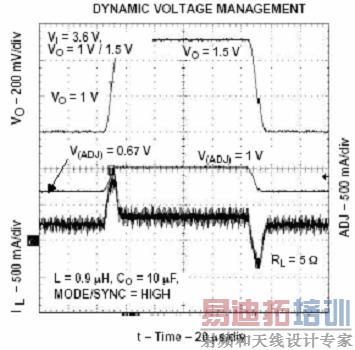
Figure 3 " Dynamic voltage management.
Powering the LCD displays
Regardless of whether an LCD display is the older dual-scan twisted nematic (DSTN) type or the high-image quality thin film transistor (TFT) type, LCD is a transmissive technology requiring a backlight. For small displays in cell phones, this backlight is provided from multiple white-light emitting diodes (wLEDs). wLEDs emit light proportional to the amount of current being driven through them. The primary weakness of this method is that the feedback loop regulates the voltage across the wLED instead of the current through the wLED. All LEDs have a non-linear V-I curve, so even the smallest change in the forward voltage of the wLED creates a change in the wLED current. As a result, older LCD displays powered by a simple boost converter had fluctuating brightness levels and little, if any, brightness control.
Since a constant, controllable forward current through a wLED delivers constant, controllable display brightness, the constant current wLED driver evolved from a simple, boost converter. The driver regulates the current through a sense resistor instead of the output voltage across the wLEDs. To prevent small leakage currents from reducing battery life during standby mode and minimize the efficiency reduction due to in-rush currents for the output capacitor start up, a wLED driver includes a load disconnect feature, which electrically removes the wLEDs from the input source when the supply is disabled. Constant current wLED drivers also require over-voltage protection in the event of an open circuit fault condition. The TPS61060 wLED driver shown in Figure 4 is an example of an inductive mode boost converter that has been customized with the features previously mentioned to operate as a wLED driver. In addition, the TPS61060 has two methods for brightness control: PWM dimming through then EN pin and digital brightness control through ILED pin. In a typical application, the TPS61060 can drive up to five wLEDs in series from a Li-Ion battery at 80 percent efficiency.

Figure 4 " Constant current wLED driver.
Passive matrix, black and white or color DSTN displays typically only require a single positive voltage rail in the 16V to 20V range, depending on the resolution and contrast ratio, which a basic, low cost boost converter can provide. Since today's smart phone displays' video imaging capabilities require high resolution and fast response times, they use active matrix thin-film-transistor (TFT) displays, which have more complex power requirements. The main difference between the passive matrix LCD bias solution and the active matrix solution is the positive and negative gate voltages that are needed to turn the TFT on and off. A third positive voltage is often required for the column driver. Depending on the system, a fourth logic supply voltage rail between 1.8 V and 3.3 V may be required for the graphic and timing controller. Configuring one or more converters to provide these voltage rails with the proper sequencing is cumbersome at best. In order to optimize the design in terms of overall solution size and efficiency, power IC manufacturers have moved to fully integrated display power solutions. TI developed the TPS65120, as shown in Figure 5, as a fully integrated display power solution providing both sequencing of the voltage rails and a separate logic supply rail.

Figure 5 - One inductor display power solution providing 4 independent voltage rails.
Expecting a Li-Ion battery input supply, the solution of Figure 5 operates with an input voltage from 2.5 V to 5.5 V. The IC provides the positive voltage VGH up to 20 V/2 mA to turn the TFT on, the negative voltage VGL down to "18 V/2 mA to turn the TFT off and the column driver voltage VMAIN, adjustable between 3.0 V to 5.6 V with 20-mA load current. An integrated LDO derives a 3.3V logic supply rail from VMAIN. Since efficiency and small solution size are key concerns, the device comes in a 3 mm 3 mm QFN package and uses a novel peak current control architecture which time multiplexes the single inductor to serve each output with exactly the right amount of power required by the load. Depending on the different input to output voltage differential and inductor, efficiencies up to 85 percent can be achieved. Most of the displays require specific power up sequencing of the different rails to assure a controlled start-up of the LCD and to avoid damages or to avoid an uncontrolled display picture. Therefore the device family has options with automatic sequencing as well as manual sequencing of each output. The solution shown in figure 5 provides sufficient output power for small displays that are used in mobile phones up to 7 inches.
Smaller phones drive power IC integration
Multi-output power ICs, like the TPS65120, are becoming more common because the latest process technologies make it much easier to combine, quickly modify, and/or leverage existing discrete IC designs. End equipment focused power IC's, like the TPS65010 shown in Figure 6, have two DC/DC converters for the higher current but lower voltage rails, two linear regulators for the low noise audio and RF control sections, integrated peripherals like ringer and buzzer controls and an I2C interface that allows dynamic voltage scaling of the converter outputs and general purpose I/Os (i.e. GPIOs).
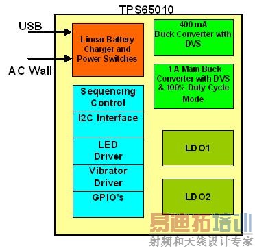
Figure 6 " Application specific multi-channel power IC .
In general, the total cost, including IC and supporting passive components cost, system design time and board space, of an integrated IC-based solution is less than solution consisting of discrete ICs. In the past, integrated ICs have been highly application specific and have not been very flexible. Therefore, they may not accommodate significant design changes late in the design cycle. However, new manufacturing process techniques, including integrated EEPROM for programming output voltage rails and post-package trimming, make "spinning" simple modifications of existing ICs (e.g., an IC with a different fixed output voltage) much simpler, faster and cheaper.
Conclusion
The increased functionality and higher performance requirements of smart phones make significant demands on the power ICs. Traditional, featureless buck and boost converters are no longer meeting those demands. Power IC manufacturers like TI are rising to the challenge by using process technology advancements to produce power ICs with unprecedented performance and application specific features. In addition, multi-channel power management ICs at various levels of integration are available to maximize battery life, in the smallest board area and at lowest cost.
射频工程师养成培训教程套装,助您快速成为一名优秀射频工程师...
天线设计工程师培训课程套装,资深专家授课,让天线设计不再难...
上一篇:如何应对便携式系统设计中提出的最新照明要求
下一篇:简单的传统得以延续――SIMPLE
SWITCHER的后续产品
射频和天线工程师培训课程详情>>