- 易迪拓培训,专注于微波、射频、天线设计工程师的培养
猜猜是什么:未充分使用的 SEPIC 性能优于反向拓扑
By John Betten and Robert Kollman, Texas Instruments, Dallas
Planet Analog
Many times designers are given a set of non-isolated supply specifications where the output voltage falls between the minimum and maximum input voltage. They then have to decide between a flyback or SEPIC (single-ended primary inductance converter) topology. The usual choice is the flyback, mostly because of lack of familiarity with the SEPIC. However, this decision may not be the best design solution.
Table 1 presents a set of electrical specifications to power an automotive stereo system. The input voltage range is quite large at 10 to 40 volts; 10 volts is provided during heavy current draw and cold conditions while a 40 volt surge can occur when the car's battery is disconnected. The output voltage of 15 volts is in the "middle" of the input voltage range, requiring a topology that can both buck and boost the input voltage. The output power is approximately 26 watts, which could generate thermal issues if the power supply is not reasonably efficient.
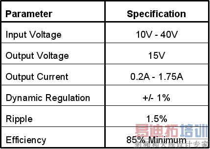
Table 1: Electrical Specifications for Typical Automotive Stereo System.
These specifications were used as the starting points to design and prototype the two candidate topologies. Figure 1 features the finished hardware. The SEPIC is on the left side and the flyback on the right. The two designs look quite similar, but the SEPIC's coupled inductor is larger than the flyback's. This larger size, and larger energy storage, is needed to keep the SEPIC converter operating in continuous-current mode (CCM) at light loads.
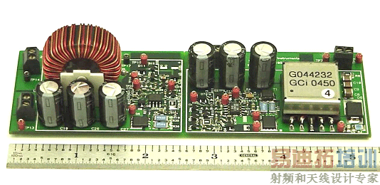
Figure 1: Demo Board (SEPIC on left side; Flyback on right).
Figure 2 presents a simplified schematic of the power stages for both topologies. In this comparison, the flyback also runs in CCM. The power switch, Q3, is turned ON to store an incremental amount of energy in the transformer. It is then turned OFF and the transformer's secondary voltage reverses. Current is forced through D6 into the output. An equal amount of energy from the transformer charges the output capacitor and is delivered to the load. Regulation is achieved by controlling the duty factor and the incremental energy into the system. Both the power-switch and diode work in unclamped inductive switching; that is, the voltage placed on them is controlled to a large degree by the transformer leakage inductance and stray capacitance.
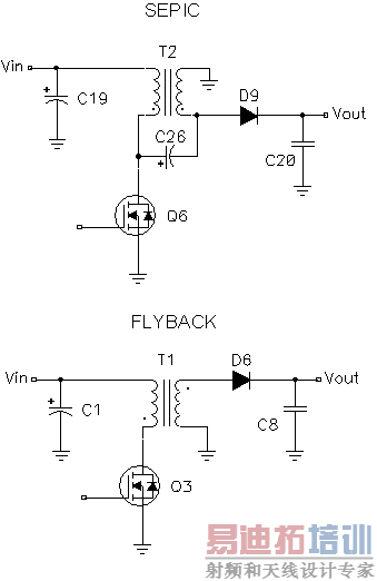
Figure 2: Simplified SEPIC and Flyback Power Supplies.
Figure 2 shows the SEPIC converter again running in CCM. When Q6 is ON, the C26 positive terminal is held at ground, while the T2 one-to-one turns ratio places a voltage equal to negative Vin on the C26 negative terminal. This means that the capacitor has the input voltage applied across it with the polarity shown. In this circuit, when the switch is turned ON, an incremental amount of energy is stored in the primary inductance. Current flows in the inductor secondary and coupling capacitor (C26) to equalize its charge. When the switch is turned OFF, the voltage on the Q6 drain rises. A current flow from both primary (through C26) and secondary (through D9) is provided to the output. This circuit has the advantage that both the FET and diode voltages are clamped by the capacitors, so there is little circuit ringing. It might seem that the SEPIC "pays a penalty" since the C26 coupling capacitor has significant ripple current. However, this ripple is offset by the much smaller ripple current from the C19 input capacitor's continuous input current. This topology has another advantage with power being simultaneously drawn from the input and delivered to the output, much like an auto-transformer. Since the power switches do not have to handle the entire power transfer, the circuit is more efficient. Table 2 compares circuit stresses between the two topologies both analytically and numerically. This table assumes a very small inductor ripple current (large inductance) and ideal diodes. It also assumes 50 percent maximum duty factor for the flyback. Capacitor ripple currents are similar for both topologies when one compares the flyback's input capacitor to the SEPIC's coupling capacitor. These capacitors should have similar voltage ratings because they are each charged to the input voltage. Both topologies have large ac ripple currents and must use low Equivalent Series Resistance (ESR) capacitors.
For this design example, the SEPIC requires a slightly larger output capacitance due to its larger duty cycle and longer diode OFF time, compared to the flyback. The table also shows FET and diode voltage stresses for both circuits. The flyback FET seems to have a lower "flat-top" stress. However, it must switch an unclamped inductance and will have significantly higher voltage stress than the SEPIC FET when this is factored in. The flyback diode Peak Inverse Voltage (PIV) starts with a larger voltage stress than that of the SEPIC, but also has an unclamped inductive-switching spike, making it significantly worse.
In this example, the voltage stress makes a Schottky diode unacceptable for the flyback and forces the use of an ultra-fast diode with its higher conduction losses and correspondingly lower efficiencies. Voltage spikes on the power switch and output diode caused by the flyback transformer leakage inductance usually require a voltage clamp and/or snubber circuit to limit the peak voltage, further reducing efficiency. FET Root Mean Square (RMS) currents are also lower with the SEPIC, decreasing on-time conduction losses relative to the flyback. The flyback's only significant component advantage is that the magnetic components tend to be smaller. The inductor's volume is roughly related to the energy storage requirement of L*I, with the flyback requiring about one-third the energy storage of the SEPIC. This energy storage accounts for the significantly larger SEPIC inductor in Figure 1.
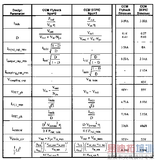
Table 2: Flyback and SEPIC Converter Design Equations (L is assumed to be Large; Diodes are Ideal).
Figures 3 and 4 show the demo circuit schematics for the prototype hardware in Figure 1. Each circuit occupies a component area of just over three square inches. The SEPIC's inductor height is twice that of the flyback's tallest component. The inductor's form factor could have been designed to lie flat to reduce height, but at the expense of increasing the PWB's area. Except for the magnetics, both designs use similar power stage components. Different controllers were chosen for each design. The flyback uses a UCC2813, which limits the duty-cycle to 50 percent maximum while the SEPIC uses a UCC3807, which allows an adjustable duty-cycle limit greater than 50 percent. In this application, it is set to a 75 percent maximum. The flyback uses three input capacitors rated to handle the large ac-RMS requirement of the pulsating current generated by the FET switch.
Generally, large-value, low-cost aluminum electrolytic capacitors work best, compared to ceramics, which don't have the capacitance necessary to provide low-input ripple voltage. In the SEPIC, only one input capacitor is required and must handle the ac-RMS rating of the triangular inductor current. This is a relatively low RMS current and capacitance value; a fairly easy requirement to meet. Two ac coupling capacitors are required on the SEPIC, which has the same stress equation as the flyback input capacitor, but is operating at a larger duty-cycle. This larger duty-cycle reduces the RMS current to two-thirds that of the flyback's input capacitors.
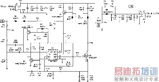
Figure 3: Flyback Converter Design.
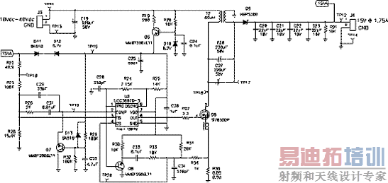
Figure 4: SEPIC Converter Design.
The waveforms in Figure 5 show the FET voltage drain present on the flyback and SEPIC circuits. The waveforms were taken at maximum output load and a 12Vdc input. The flyback transformer leakage inductance produces a voltage spike that adds an additional 20V to the "flat-top" voltage. In comparison, the SEPIC FET switching waveform is clamped, and shows very little overshoot, or ringing. This clamping results in less switching-loss, output voltage noise and a power stage that can be operated at a much higher frequency than that of the flyback.
Figure 6 shows the flyback and SEPIC output diode switching waveforms. Again, the flyback transformer leakage inductance produces a significant voltage spike relative to the SEPIC. A 200V output diode is required for the flyback to handle the large negative ringing compared to the SEPIC's 60V Schottky diode. The 0.5 volt forward drop of the SEPIC's Schottky diode relative to the one volt forward drop of the flyback's ultra-fast diode, results in significant power savings for the SEPIC.
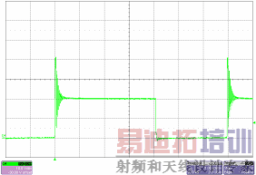
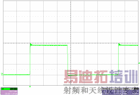
Figure 5: Power FET Drain Waveforms (10V/div) (Top: Flyback; Bottom: SEPIC).
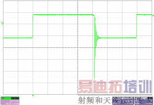
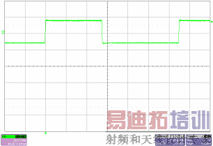
Figure 6: Output Diode Waveforms (20V/div) (Top: Flyback; Bottom: SEPIC).
Figure 7 shows the efficiency of both circuits measured at two input voltages. The SEPIC generally achieves four percent higher efficiency overall than that of the flyback circuit, reaching a peak efficiency of 92.7 percent. Component dissipations are similar for both circuits, except for the output diode and snubbers. It is the unclamped inductive- switching that forces the use of a higher voltage diode, consequently resulting in higher losses as well as requiring the use of snubbers.
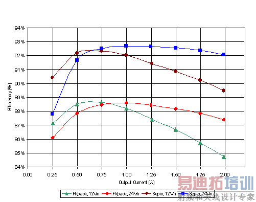
Figure 7: SEPIC Provides Better Efficiency than Flyback Converter.
While the flyback converter's relative simplicity and familiarity has its advantages, the SEPIC converter can provide higher efficiency and lower component stress. Table 3 compares the two approaches. The SEPIC is more efficient due to lower FET and diode stresses. The flyback has lower component area since the SEPIC has larger magnetics. Component count is similar for the two designs, with an equal number of power components and similar number of support components. The flyback has the disadvantage of requiring snubbers. Continuous input current not only reduces ripple current rating of the SEPIC's input capacitor, but also helps improve a system's electromagnetic emissions. If there are other loads on the 12 volt input, the flyback's discontinuous input current is more likely to generate an unacceptable ripple on the input, requiring additional filtering.
An additional consideration involves the understanding of the control loop characteristics. Compared to the flyback, the SEPIC control loop characteristics are much less documented and not generally understood. A SEPIC operating in CCM and implementing current mode control, as presented, can present control loop challenges. This involves compensating for a right half-plane zero and wide variations in closed-loop gain over input voltage and output loading. This can result in lower control loop gain, which can degrade transient load performance. However, when implemented correctly, the SEPIC converter provides an excellent, high-efficiency solution.
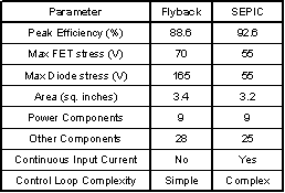
Table 3: SEPIC can offer significant advantages over flyback.
射频工程师养成培训教程套装,助您快速成为一名优秀射频工程师...
天线设计工程师培训课程套装,资深专家授课,让天线设计不再难...
上一篇:采用箝位电路抑制车载电压瞬变
下一篇:如何实现便携式系统设计中最新提出的照明要求

