- 易迪拓培训,专注于微波、射频、天线设计工程师的培养
PADS中应该注意的一个问题.
录入:edatop.com 点击:
pads 2005 LAYOUT
tools-options-design-drill
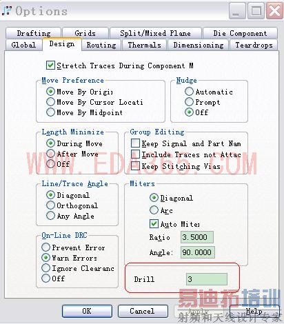
Specifying Copper Plating Thickness for Drill Holes
Use the Drill Oversize box to specify the amount of space that PADS Layout automatically adds to plated drill holes to account for copper plating inside drill holes. This amount of space is called drill oversize. The drill size plus the drill oversize equals the finished NC drill size diameter. CAM outputs for NC drill reflect the finished size value.
Drill oversize also applies to plated via and pin drill holes. You specify whether a via or pin is plated in the Pad Stack Setup dialog box.
tools-options-design-drill
Specifying Copper Plating Thickness for Drill Holes
Use the Drill Oversize box to specify the amount of space that PADS Layout automatically adds to plated drill holes to account for copper plating inside drill holes. This amount of space is called drill oversize. The drill size plus the drill oversize equals the finished NC drill size diameter. CAM outputs for NC drill reflect the finished size value.
Drill oversize also applies to plated via and pin drill holes. You specify whether a via or pin is plated in the Pad Stack Setup dialog box.
TOOLS-->OPTIONS-->DESIGN的DRILL中改为0
呵呵,楼主英语水平不错!
Specifying Copper Plating Thickness for Drill Holes
此參數表示過孔的電鍍厚度,不能為0吧.
9 W0 t9 ]4 `/ c4 c; Y( U# w! ]
請指點,為何為零?
指点一下啊
那个不能为零,表电镀厚度
又学习了一下谢谢
这个决对不能改为0,否则PTH发孔就没法做了
射频工程师养成培训教程套装,助您快速成为一名优秀射频工程师...
天线设计工程师培训课程套装,资深专家授课,让天线设计不再难...
上一篇:菜鸟求助-添加元件的某个问题?
下一篇:问一个PADS的安装问题
射频和天线工程师培训课程详情>>