- 易迪拓培训,专注于微波、射频、天线设计工程师的培养
CAT6500自动电源选择开关详细介绍
录入:edatop.com 点击:
CAT6500 is an automatic power switch designed to select between two power sources and direct that power to a load for battery charging or system power.
CAT6500’s power inputs withstand voltages of up to 18 V and protect the downstream load from voltages exceeding 7V. In the event of a polarity reversal at either input CAT6500’s internal power switches will shut off to prevent discharge of the system’s internal power source.
功能框图:
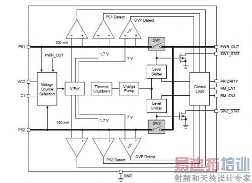
CAT6500功能框图
管脚定义:
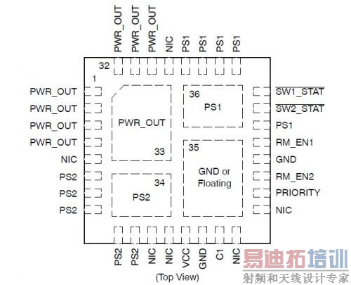
CAT6500管脚定义
引脚功能描述:
| Pin No. | Pin Name | Description |
|
| 1, 2, 3, 4 | PWR_OUT | Power Output. Must be tied to PWR_OUT on opposite side of chip. Use all 3 pins each side. |
|
| 5 | NIC | No Internal Connection. A signal or voltage applied to this pin will have no effect on device operation. |
|
| 6, 7, 8, 9, 10 | PS2 | Power Source #2. External power input |
|
| 11, 12 | NIC | No Internal Connection. A signal or voltage applied to this pin will have no effect on device operation. |
|
| 13 | VCC | Power input from battery. |
|
| 14 | GND | Ground. Reference point for all voltages. |
|
| 15 | C1 | Filter capacitor for CAT6500’s internal power bus |
|
| 16 | NIC | No Internal Connection. A signal or voltage applied to this pin will have no effect on device operation. |
|
| 17 | NIC | No Internal Connection. A signal or voltage applied to this pin will have no effect on device operation. |
|
| 18 | PRIORITY | Priority selects preferred power source when both PS1 and PS2 are powered. |
|
| 19 | RM_EN2 | Reverse Mode Enable 2. Overrides PRIORITY and turns SW2 ON. |
|
| 20 | GND | Ground. Reference point for all voltages. |
|
| 21 | RM_EN1 | Reverse Mode Enable 1. Overrides PRIORITY and turns SW1 ON. |
|
| 22 | PS1 | Power Source #1. External power input. |
|
| 23 |
SW2_STAT | Power Source 2 Status. An open drain LOW true logic level output indicating that the switch SW2 is |
|
|
| |||
| 24 |
SW1_STAT | Power Source 1 Status. An open drain LOW true logic level output indicating that the switch SW1 is |
|
|
| |||
| 25, 26, 27, 28 | PS1 | Power Source #1. External power input. |
|
| 29 | NIC | No Internal Connection. A signal or voltage applied to this pin will have no effect on device operation. |
|
| 30, 31, 32 | PWR_OUT | Power Output. Must be tied to PWR_OUT on opposite side of chip. Use all 3 pins each side. |
|
| 33 | PWR_OUT | Electrically active thermal pad. Does not need to be connected to other PWR_OUTs. Can be left float-ing but must not be connected to other signal paths or Ground. |
|
| 34 | PS2 | Electrically active thermal pad. Does not need to be connected to other PS2 pins. Can be left floating but must not be connected to other signal paths or Ground. |
|
| 35 | – | Mechanical support for control IC. This chip does not generate any significant heat and does not need a separate heat sinking connection. Electrically this may be left floating or can be grounded. It should NOT be connected to other signals or voltages. |
|
| 36 | PS1 | Electrically active thermal pad. Does not need to be connected to other PS1 pins. Can be left floating but must not be connected to other signal paths or Ground. |
|
CAT6500技术方案、应用案例、电路图集锦
涵盖了CAT6500的技术方案和CAT6500的应用笔记以及CAT6500的电路图,为工程师学习CAT6500提供了一站式学习环境。
射频工程师养成培训教程套装,助您快速成为一名优秀射频工程师...
射频和天线工程师培训课程详情>>