- 易迪拓培训,专注于微波、射频、天线设计工程师的培养
ZMDI ZSSC1856双路智能电池管理解决方案
录入:edatop.com 点击:
ZMDI公司的ZSSC1856是集成了嵌入式MCU的双路ADC,有两个芯片组成,PQFN32 5x5mm封装.系统基本芯片(SBC)包含了高压电路,LIN收发器以及包括外设,18位ΣΔ-ADC,数字滤波在内的确模拟输入级.MCU芯片包括MCU核,存储器和一些外设.MCU和SBC的通信由SPI接口处理.正常模式的电流为10mA-20mA,低功耗模式小于100uA,主要用在汽车的智能电池检测,需要精密电池的工业和医疗应用.本文介绍了ZSSC1856主要特性,方框图,SBC数字部分和MCU部分方框图以及典型应用电路.
The ZSSC1856 is a dual-channel ADC with an em-bedded microcontroller for battery sensing/management in automotive, industrial, and medical systems.
The ZSSC1856 consists of two silicon dies in one package. The dies are assembled as stacked dies in a PQFN32 5x5mm package. The System Basis Chip (SBC) contains the high voltage circuits, the analog input stage including peripheral blocks, the ΣΔ-ADCs, the digital filtering, and the LIN-transceiver. The microcontroller chip (MCU) contains the microcontroller core, memories, and some peripheral blocks. Communication between the MCU and the SBC is handled by an SPI interface. Internal nodes connecting the MCU and the SBC (i.e., TXD, RXD, IRQN, CSN, SPI_CLK, MOSI, MISO, MCU_CLK, MCU_RSTN, and RAM_PROTN) are controlled by firmware. Users can access the internal nodes via the LIN interface and/or external JTAG pins (i.e., TDO, TDI, TRSTN, TMS, and TCK).
One of the two input channels measures the battery current IBAT via the voltage drop at the external shunt resistor. The second channel measures the battery voltage VBAT and the temperature. An integrated flash memory is provided for customer-specific soft-ware; e.g., dedicated algorithms for calculating the battery state.
During Sleep Mode (e.g., engine off), the system makes periodic measurements to monitor the dis-charge of the battery. Measurement cycles are controlled by the software and include various wake-up conditions. The ZSSC1856 is optimized for ultra-low power consumption and draws only 100μA or less in this mode.
ZSSC1856主要特性:
High-precision 18-bit sigma-delta ADC with on-chip voltage reference (5ppm/K)
Current channel
IBAT offset error: ≤ 10mA
IBAT resolution: ≤ 1mA
programmable gain: 4 to 512
Differential input stage input range: ± 300mV
Sampling rate: 1Hz to 16kHz
Voltage channel
Input range: 4 to 28.8V
Voltage accuracy: ± 2mV
Temperature channel
Internal temperature sensor: ± 2℃
External temperature sensor (NTC)
On-chip precision oscillator (1%)
On-chip low-power oscillator
ARM® Cortex™-M0* microcontroller: 32-bit core, 10MHz to 20MHz
96kB Flash/EE Memory with ECC, 8kB SRAM
LIN2.1 / SAE J2602-1 Transceiver
Directly connected to 12V battery supply
Current consumption
Normal Mode: 10mA to 20mA
Low-Power Mode: ≤ 100μA
ZSSC1856优势:
Integrated, precision measurement solution for accurate prediction of battery state of health (SOH), state of charge (SOC) or state of function (SOF)
Flexible wake-up modes allow minimum power consumption without sacrificing performance
No temperature calibration or external trimming components required
Optimized code density through small instruction set architecture Thumb®-2 *
Robust POR concept for harsh automotive environments
Industry’s smallest footprint allows minimal module size and cost
AEC-Q100 qualified solution
Physical Characteristics
Wide operation temperature: -40℃ to +125℃
Supply voltage: 4.2 to 18 V
Small footprint package: PQFN32 5x5 mm
ZSSC1856应用:
Intelligent battery sensing for automotive applications; e.g., start/stop systems, e-bikes, scooters, and e-carts
Industrial and medical applica-tions requiring precise battery SOC, SOH and SOF monitoring; e.g., emergency lighting, uninter-ruptable power supplies, hospital equipment, alarm systems, and more.
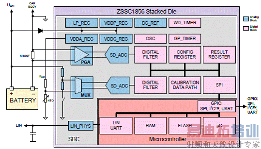
图1.ZSSC1856方框图
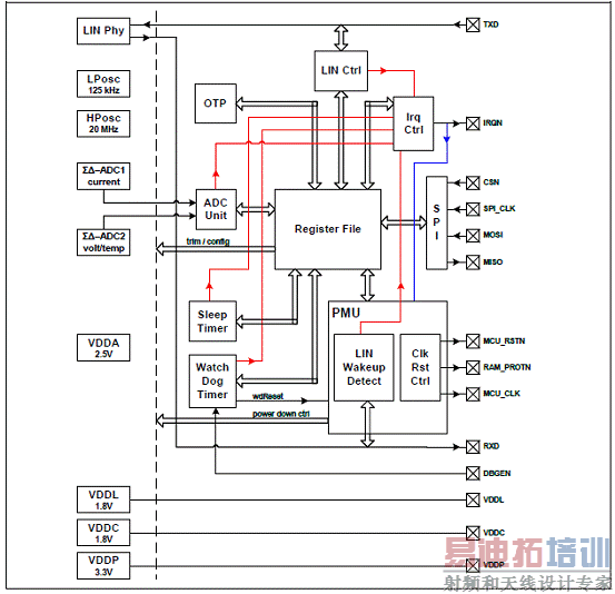
图2.ZSSC1856 SBC数字部分方框图
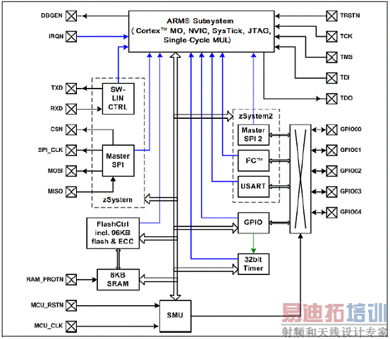
图3.ZSSC1856 MCU部分方框图
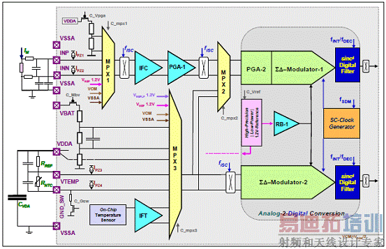
图4.ZSSC1856模拟测量子系统功能框图
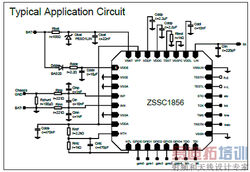
图5.ZSSC1856典型应用电路图
详情请见:
http://www.zmdi.com/products/sensor-signal-conditioner/zssc1856/
来源:网络
The ZSSC1856 is a dual-channel ADC with an em-bedded microcontroller for battery sensing/management in automotive, industrial, and medical systems.
The ZSSC1856 consists of two silicon dies in one package. The dies are assembled as stacked dies in a PQFN32 5x5mm package. The System Basis Chip (SBC) contains the high voltage circuits, the analog input stage including peripheral blocks, the ΣΔ-ADCs, the digital filtering, and the LIN-transceiver. The microcontroller chip (MCU) contains the microcontroller core, memories, and some peripheral blocks. Communication between the MCU and the SBC is handled by an SPI interface. Internal nodes connecting the MCU and the SBC (i.e., TXD, RXD, IRQN, CSN, SPI_CLK, MOSI, MISO, MCU_CLK, MCU_RSTN, and RAM_PROTN) are controlled by firmware. Users can access the internal nodes via the LIN interface and/or external JTAG pins (i.e., TDO, TDI, TRSTN, TMS, and TCK).
One of the two input channels measures the battery current IBAT via the voltage drop at the external shunt resistor. The second channel measures the battery voltage VBAT and the temperature. An integrated flash memory is provided for customer-specific soft-ware; e.g., dedicated algorithms for calculating the battery state.
During Sleep Mode (e.g., engine off), the system makes periodic measurements to monitor the dis-charge of the battery. Measurement cycles are controlled by the software and include various wake-up conditions. The ZSSC1856 is optimized for ultra-low power consumption and draws only 100μA or less in this mode.
ZSSC1856主要特性:
High-precision 18-bit sigma-delta ADC with on-chip voltage reference (5ppm/K)
Current channel
IBAT offset error: ≤ 10mA
IBAT resolution: ≤ 1mA
programmable gain: 4 to 512
Differential input stage input range: ± 300mV
Sampling rate: 1Hz to 16kHz
Voltage channel
Input range: 4 to 28.8V
Voltage accuracy: ± 2mV
Temperature channel
Internal temperature sensor: ± 2℃
External temperature sensor (NTC)
On-chip precision oscillator (1%)
On-chip low-power oscillator
ARM® Cortex™-M0* microcontroller: 32-bit core, 10MHz to 20MHz
96kB Flash/EE Memory with ECC, 8kB SRAM
LIN2.1 / SAE J2602-1 Transceiver
Directly connected to 12V battery supply
Current consumption
Normal Mode: 10mA to 20mA
Low-Power Mode: ≤ 100μA
ZSSC1856优势:
Integrated, precision measurement solution for accurate prediction of battery state of health (SOH), state of charge (SOC) or state of function (SOF)
Flexible wake-up modes allow minimum power consumption without sacrificing performance
No temperature calibration or external trimming components required
Optimized code density through small instruction set architecture Thumb®-2 *
Robust POR concept for harsh automotive environments
Industry’s smallest footprint allows minimal module size and cost
AEC-Q100 qualified solution
Physical Characteristics
Wide operation temperature: -40℃ to +125℃
Supply voltage: 4.2 to 18 V
Small footprint package: PQFN32 5x5 mm
ZSSC1856应用:
Intelligent battery sensing for automotive applications; e.g., start/stop systems, e-bikes, scooters, and e-carts
Industrial and medical applica-tions requiring precise battery SOC, SOH and SOF monitoring; e.g., emergency lighting, uninter-ruptable power supplies, hospital equipment, alarm systems, and more.

图1.ZSSC1856方框图

图2.ZSSC1856 SBC数字部分方框图

图3.ZSSC1856 MCU部分方框图

图4.ZSSC1856模拟测量子系统功能框图

图5.ZSSC1856典型应用电路图
详情请见:
http://www.zmdi.com/products/sensor-signal-conditioner/zssc1856/
来源:网络
射频工程师养成培训教程套装,助您快速成为一名优秀射频工程师...
天线设计工程师培训课程套装,资深专家授课,让天线设计不再难...
上一篇:USB充电解决方案:高效AC适配器
下一篇:涡轮加速升压
(Turbo-boost)
充电器可为CPU涡轮加速模式提供支持
射频和天线工程师培训课程详情>>

