- 易迪拓培训,专注于微波、射频、天线设计工程师的培养
LOGi FPGA 开发板:可在树莓派和Beaglebone上开发FPGA
录入:edatop.com 点击:
最近在Kickstarter网站上,Valent F(x)团队正在为LOGi FPGA开发板的生产筹备资金。
LOGi 是fpga开发与arm平台的结合。Valent F(x)团队开发了可以支持树莓派和Beaglebone上开发的FPGA开发板,LOGi系列。它让FPGA开发与入门变得简单,同时趋于统一现存硬件接口和开源开发平台,如树莓派和Beaglebone Black这两个流行的开源开发平台。
Valent F(x)团队分别针对树莓派和Beaglebone Black开发了两个版本的LOGi板,如下图的LOGi-Pi和LOGi-Bone。LOGi-Pi的FPGA板的底部连接器可与树莓派的GPIO头连接,LOGi-Bone的FPGA板有两行的连接器可与Beaglebone Black 2x46引脚头相连接。不需要JTAG或者繁杂的命令,只需要在树莓派或者Beaglebone Black平台的终端输入logi_loader.bit,就可以运行LOGi板。
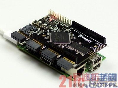
LOGi-Pi for the Raspberry Pi
LOGi-Pi 的基本技术参数:
Xilinx Spartan 6 LX9 FPGA 9,152 Logic Cells, 16 DSP48A1 Slices, 576Kb RAM
Plug-and-Play Interfacing for the Raspberry Pi 4 Layer Optimized Design to Support Maximum Performance of High Bandwidth Applications Length-tuned GPMC, SDRAM, LVDS Signals
3.3V I/O Regulator and 1.2V Core Regulator
256 Mb SDRAM connected to the FPGA
2x LEDs 2x Push Buttons 2x DIP Switches
1x High Bandwidth SATA connector expansion, port Length tuned and impedance routed differential signals for maximum bandwidth (Designed for modular LVDS expansion, Not SATA devices - see FAQ on SATA connector)
2x Digilent Inc. PMOD ports supporting 59+ plug-and-play hardware modules
1x Arduino compatible headers connected to the FPGA pins (3.3V only) Supports over 200+ Arduino Shield Modules
10x Length-tuned LVDS Pairs 32 FPGA I/O available through PMOD and Arduino headers
Connection to the SPI Interface of the Raspberry Pi (3.8 MBps maximum Bandwidth)
Connection to 16 I/O of the Raspberry Pi expansion port (including SPI, UART, I2C and GCLK and GPIO).
Bit-Stream loading interface connected to the host processor, optional bitstream FPGA self-loading from onboard Flash.
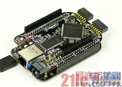
LOGi-Bone for the Beaglebone
LOGi-Bone的基本技术参数:
Xilinx Spartan 6 LX9 TQFP-144 FPGA 9,152 Logic Cells, 16 DSP48A1 Slices, 576Kb RAM
Beaglebone Black Optimized 4 Layer Optimized Design to Support Maximum Performance of High Bandwidth Applications Length-tuned GPMC, SDRAM, LVDS Signals 3.3v I/O Regulator and 1.2v Core
Regulator 256 Mb SDRAM connected to the FPGA
2x LEDs 2x Push Buttons 2x DIP Switches
1x High Bandwidth SATA connector expansion port, Length tuned and impedance routed differential signals for maximum bandwidth (Designed for modular LVDS expansion, Not SATA devices - see FAQ on SATA connector)
2x Digilent Inc. PMOD ports supporting 59+ plug-and-play hardware modules
1x Arduino compatible headers connected to the FPGA pins (3.3V only) Supports over 200+ Arduino Shield Modules
Optional GPMC, SPI or I2C port access from the Beaglebone Black
10x Length-tuned LVDS Pairs
Bit-Stream loading interface connected to the host processor, optional bitstream FPGA self-loading from onboard Flash.
射频工程师养成培训教程套装,助您快速成为一名优秀射频工程师...
天线设计工程师培训课程套装,资深专家授课,让天线设计不再难...
上一篇:电子设计发展趋势
―
开源PCB设计
下一篇:三种布局的半桥谐振变换器的分析研究
射频和天线工程师培训课程详情>>