- 易迪拓培训,专注于微波、射频、天线设计工程师的培养
Dracula LVS介绍
录入:edatop.com 点击:
Dracula lvs command file的编写相对于其他几项来说较为容易点,重点部分就是节点信息的传输与器件的识别上。本篇前一部分讲解常用的LVS命令,后一部分是实例分析与具体的编写的技术文档。
定义器件及器件:
ELEMENT MOS {[type]} layer-a layer-b layer-c {layer-d};;device layer+g+s/d+sub
ELEMENT CAP {[type]} layer-a layer-b layer-c {layer-s}
ELEMENT RES {[type]} layer-a layer-b {layer-d}
ELEMENT BJT {[type]} layer-a layer-b layer-c layer-d {layer-s}
ELEMENT DIO {[type]} layer-a layer-b layer-c {layer-s}
ELEMENT LDD {[type]} layer-a layer-b layer-c layer-d {layer-e}
ELEMENT PAD {[type]} layer-a layer-b
ELEMENT device layer-a layer-b {layer-c} {layer-d} {layer-e}
这些命令用来组合不同类型的器件,以device layer开始,接着说明器件的terminals,为了识别特殊的器件,还会常用到select 命令,比如lab[r] dio , cut res等用法。
设定参数:
Parameter res /cap {[type]} value1 {value2}
该命令类似lpe的attribute ,其中cap有value1, value2 以说明面积及边长对电容值的影响。
节点信息传输命令:
Lvs对比主要是节点信息传输的过程,在connect-layer中从下到上说明可用于传导的层次,并且在使用and, not命令时会自动传递信息。使用connect命令来说明层次间的传递。使用stamp命令使用在没有在connect/ connect-layer中说明的层的信息传递。
Connect layer-a layer-b BY cont-layer
Stamp stamped-layer by stamping-layer {output {[option]} c-name l-num {d-num}}
Connect-layer = layer1 layer2 …
实例操作:
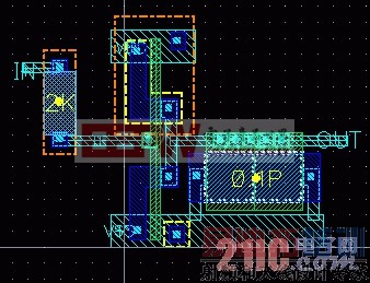
延续上次LPE中的实例,增加了电阻与电容以增加器件的比对,其中lvs_test.cir为spice netlist,lvs_test为layout cell, lvs.com为这次实例所编写的命令文件 。编写的文件中,使用的*.resval, *.capval 及lvschk 选项resval, capval对比电阻、电容的值,增加lvschk[p] 增加电容端点顺序的对比。版图中电阻为nwell电阻加res层进行识别,电容为gate电容加dummy层进行识别。
Lvs_test.cir
*** SPICE file subckt lvs_test ****
.param
.global vss vdd
*.bipolar
*.resval
*.capval
[p]
******************************************
******************************************
.subckt inv1 op ip
mi31 op ip vss vss n l=0.65u w=1.25u
mi32 op ip vdd vdd p l=0.65u w=1.25u
.ends
******************************************
******************************************
.subckt lvs_test out in
r01 in net01 2k $[rs]
x02 out net01 inv1
c03 out vss 0.1p $[cp]
.ends
******************************************
******************************************
以下为lvs command file的具体内容,需要着重注意的是connect, connect-layer及stamp命令,并区分器件层与传输层的关系,也因此可以发现nwell,gate都作了区别。
Lvs.com
;;++++++++++++++++++++++++
;;+ TOOL : dracula 4.8 +
;;+ TITLE:LVS CMD TEST +
;;+ CELL : LVS_TEST +
;;+ AUTHOR: NFMAO +
;;+ DATE : 2005-05-11 +
;;+ FROM: www.chalayout.com +
;;+++++++++++++++++++++++++
*des
primary = lvs_test
indisk = ../db/lvs_test.db
;outdisk = test.gds
printfile = lvs_test
system = gds2
resolution = 0.005 mic
scale = 0.001 mic
mode = exec now
listerror = yes
program-dir = $drac/
keepdata = inquery;yes;smart
error-path-wid = 5.0 mic
check-path = center-line
summary-only = yes
; cnames-csen = yes
; text-pri-only = yes
text-level = 0
status-command = time;du
abort-p-g-short = yes;no;all
power-node = VDD,vdd
ground-node = VSS,vss
schematic = loglvs/lvs_test.s
model = mos[n],n mos[p],p
*end
[p]
*input-layer
pldd = 1
contac = 3
mt1 = 4 text 4 texttype 0 attach mt1
thinox = 5
nwell = 6 text 7 attach rnwel
res = 7
poly = 8
dummy = 16
substrate = bulk 99
connect-layer = psub anwel pdiff ndiff poly mt1
*end
*oper
not bulk nwell psub
and poly thinox gate
and gate dummy cgate
not gate cgate agate
and agate pldd pgate
not agate pldd ngate
not thinox gate diff
and diff pldd pdiff
not diff pdiff ndiff
;and contac pdiff pcont
;and contac ndiff ncont
sel nwell cut res rnwel
not nwell rnwel anwel
and rnwel res wres
not rnwel wres wress
and psub pdiff pcont
and anwel ndiff ncont
[p]
connect mt1 poly by contac
connect mt1 pdiff by contac
connect mt1 ndiff by contac
connect ndiff anwel by ncont
connect pdiff psub by pcont
stamp wress by ndiff
element res[rs] wres wress
parameter res[rs] 1000
element cap[cp] cgate poly ndiff
parameter cap[cp] 5.5e-15 1.0e-17
element mos[n] ngate poly ndiff psub
element mos[p] pgate poly pdiff anwel
lvschk[rsp] printline=1000 lper=0 wper=0 resval=0 capval=5
*end
射频工程师养成培训教程套装,助您快速成为一名优秀射频工程师...
射频和天线工程师培训课程详情>>