- 易迪拓培训,专注于微波、射频、天线设计工程师的培养
Backdrill相关设置及Backdrill文档输出方法
录入:edatop.com 点击:
如果PCB的层数超过4层,PCB的走线从其中的某两层走线(除从表层到表层外),总会产生类似于下图这种情形的stub:产生多余的镀铜部分,当电路信号的频率增加到一定高度后,多余的镀铜就相当于天线一样,产生信号辐射对周围的其他信号造成干扰,严重时将影响到线路系统的正常工作,Backdrill的作用就是将多余的镀铜用钻孔的方式钻掉,从而消除此类EMI问题。其操作步骤和注意事项如下: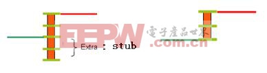
1.给net设定Backdrill_max_pth_stub属性
Property | BACKDRILL_MAX_PTH_STUB |
Purpose | Identification of nets targeted for backdrilling |
Usage | Required |
Value | Max allowable stub in length (database units) |
Objects | Nets |
Backdrill analysis flag | S |
2.给net设定Backdrill_min_pin_pth属性, Backdrill_min_pin_pth 考虑可靠性, 必须保证BACKDRILL去掉多余镀铜 后, 保证一定剩余一定长度. 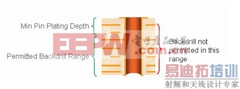
Property | BACKDRILL_MIN_PIN_PTH |
Purpose | Ensures minimum pin plating depth is not compromised |
Usage | Optional |
Value | Length |
Objects | Symbols, pins |
Backdrill analysis flag | P |
3.压接的接插件backdrill:要保证良好的接触, 必须保证下面的值: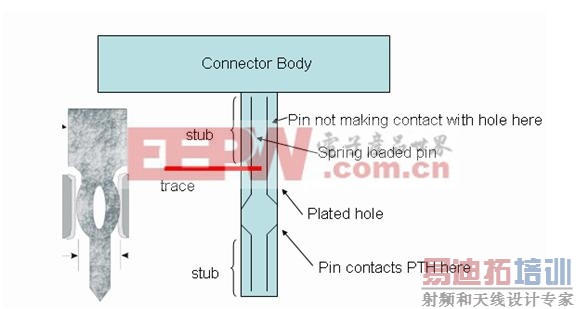 [p]
[p]
Property | BACKDRILL_PRESSFIT_CONNECTOR |
Purpose | Use on pressfit connectors to permit backdrilling from both sides of the board. Backdrill depth will not protrude into contact range as defined by the property string. |
Usage | Optional |
Value | value1:value2> where values = pin contact range; this value must be obtained from the manufacturer |
Objects | Symbols |
Backdrill analysis flag | n/a |
4.有些场合不能用此功能的可以用下面的命令排除.
Exclusions
It may be necessary to exclude certain objects from backdrilling even though stub violations are present. The BACKDRILL_EXCLUDE property can be applied to symbols, pins or vias at both the library and design level using Edit - Property. Common examples might include solder tail connectors or a dense pin escape pattern in BGA areas. The PCB designer should consult with a manufacturing engineer before assuming all pin/via objects are suitable for backdrilling.
Property | BACKDRILL_EXCLUDE |
Purpose | Excludes objects from backdrilling even though stub may be present |
Usage | Optional |
Value | Boolean (true/false) |
Objects | Symbols, pins, vias |
Backdrill analysis flag | X |
[p]
5.定义层(可选)
User Overrides
In most cases, the backdrill layer ranges defined in the Backdrill Setup and Analysis user interface satisfy your requirements to manage stubs. The BACKDRILL_OVERRIDE property allows user-specified control of layer ranges for any pin or via and from ether side of the board or both. This is done regardless of violations that may result, such as testpoint conflicts or backdrilling through a connection. The override property was considered for the design of test coupons where the OEM wishes to evaluate the performance of the board fabricator with respect to the adherence of depth ranges. The designer may override the to layer to effectively drill out the layer where the trace connects the pin/via. The expected usage of this property is limited; please exercise caution to prevent accidental over-drilling.
Property | BACKDRILL_OVERRIDE |
Purpose | User-specified backdrill range |
Usage | Optional: special circumstances |
Value | TOP:layer_name>:BOTTOM:layer_name> |
Objects | Pins, Vias |
Backdrill analysis flag | O or W (warning) |
定义方法:在Manufacture>NC …Backdrill setup and analysis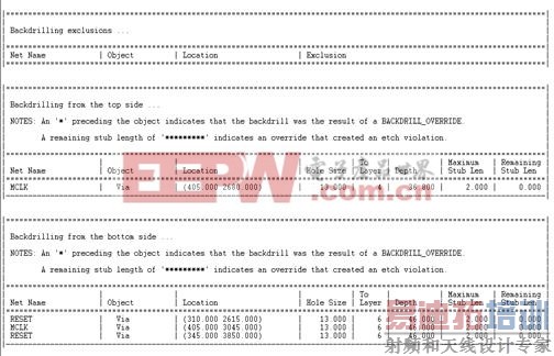
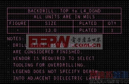
6.NC>DRILLLENGEND,输出钻孔表,注意要选择 Include backdrill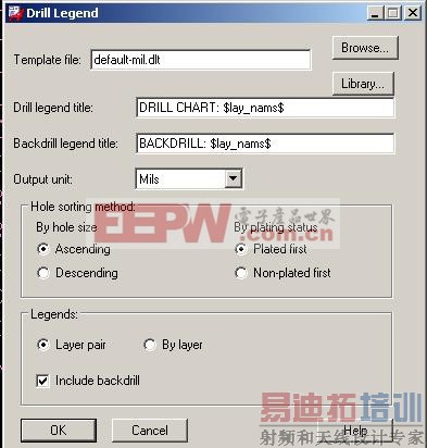 >
> 
7.产生钻孔文件,输出钻孔文件,也要s Include backdrill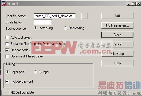
射频工程师养成培训教程套装,助您快速成为一名优秀射频工程师...
天线设计工程师培训课程套装,资深专家授课,让天线设计不再难...
上一篇:光电PCB技术简介
下一篇:过阻尼与欠阻尼的问题探讨
射频和天线工程师培训课程详情>>