- взЕЯЭиХрбЕ,зЈзЂгкЮЂВЈЁЂЩфЦЕЁЂЬьЯпЩшМЦЙЄГЬЪІЕФХрбј
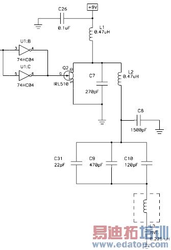
13.56MHz PA for RFID reader reference design.
For the power amplifier, how to design the matching network? how to decide the component value?
In this PA design, the value of RF chock L1 is not large (0.47 uH), actually it has the same value as L2. Why? Also, C9, C10 and C31 are connected in parallel, why is that? To my understanding, several caps connected in parallel is to provide a wide bandwidth low impedance signal path, small cap has higher self resonance frequence (SRF). But I don't think the SRF of capacitor in pF range has effect at 13.56MHz, why are they connecting caps like that?
I can download the Spice model of the power MOSFET IRL510 from International Rectifier and import it to ADS, but how to design the PA using this model and end up with this design? Should I start with simulating the load pull contour?
Thank you.
13.56_mhz_rfid_reader_1511.pdf (71.5 KB)
Of course, this is not a reader but a transmitter.
Just a guess, but L1 is not an RF choke but is instead part of the antenna circuit.
The three capacitors in series have staggered values so you can possilby "tune" the antenna by removing one of two of them?
An RFID reader includes a transmitter and a receiver.
Yes L1 is not an RF chock. After I read some power amplifier design, I think this is a class E PA. L1 and the MOS drain capacitance (including C1) resonance at the operation frequency (13.56MHz).
But I still can not understand the other part of the PA. From the attached application note of "The Handiman's Guide to MOSFET 'Switched Mode' Amplifiers", the author presented two types class E PA: the typical and series tuned PA. But the reference design belongs to none of them. I can not understand the connection of L2 and C8. Can somebody tell me why they connect like that? And why C8 has such a large capacitance?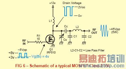
class-e2_6531.jpg (272.3 KB)
Another quesiton:
We use class E PA because it can provide higher efficiency. But if the load is an inductor such as a coil antenna. Ideally it has no power loss at the load. In this case how to calculate the efficiency?
The load is not just inductor - it is tuned to working frequency .All capacitors and chokes are used to - filter harmonics and match the pcb antenna impedance to PA output impedance .
Regarding 3 capacitors usage , i suppose it is to get final capacitor value to tune pcb antenna choke which is fixed topology (you have to repeat coil exactly as in AN or adjust output passive stage to new coil parameters).
Yet i remember in old days parallel capacitors used for thermocompensation when all component temco and values selected to keep coil tuned over temperature range (used in oscillators). But i guess it is not the case in this application.
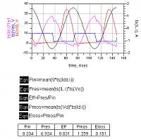
I did some simulation on ADS. I import the MOS model of IRF510 from international rectifier. After tuning, I got a efficiency of 83% out of the PA. The load is 5 Ohm.
Is my testing setup correct?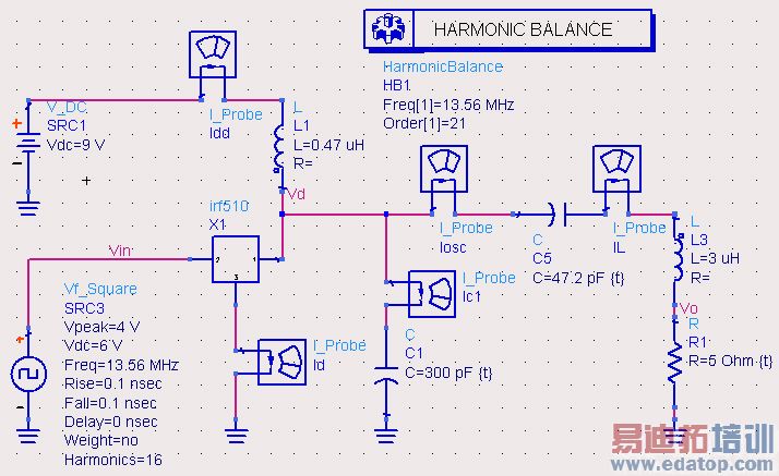
Hi yolande_yj,
Because the PA is a Class-E amplifier, you may use a specific, free software to get components value, see this link:
http://tonnesoftware.com/classe.html
Of course you have to figure out approximate output power from the 9V supply for a selected resistive load (see below) with the given L1 and L2 and C7 values.C8, C9, C10, C31 and L3 seems a capacitively tapped resonant circuit,(L3 is the antenna loop for the PA) and obviously has a real (not reactive) load of a certain value towards the PA at 13.56MHz resonant frequency.How much real load it may represent could be figured out from the capacitive divider formula, using a Q quality factor of around 30-35 for L3 to estimate its resonant impedance.
Here is the link to the Microchip application note on this topic you probably took the READER SCHEMATICS which includes the PA circuit too (PDF page 151):
http://ww1.microchip.com/downloads/e...doc/21299e.pdf It includes some useful info on almost everything needed here.
Probably this is a coincidence only, and the indeed low value of L1 was chosen to dissipate some power from the output by shunting the drain-source through the supply's path?Maybe...
Probably to make the tuning/adjusting the PA output power within specification / compensate for the tolerance in the antenna L3, I guess. Using paralleled caps in PAs is also to reduce ESR dissipation in them (as you hinted at) but here it is not really justified due to the (low) frequency and the output power.
I think your simulation in ADS is ok but you used different values with respect to the original design. If you could repeat the HB simulation with exactly the same schematics shown in your first post here, it would be more beneficial for you I think.
Use a load resistor at L3 which comes from the Q=35 @ 13.56MHz for L3=0.225uH. (r=XL/Q). Of course the parallel equivalence of this series load resistor will be transformed to the PA by the capacitive dividers of (C9+C10+C31) and C8.And include a single cap of 612pF for C9+C10+C31 in your simulation.
I believe this way you can more exactly approach this PA design. Hope what I included is understandable.
regads
unkarc
FYI:
The Handiman's Guide to MOSFET "Switched Mode" Amplifiers:
Part 1,
Part 2
you can find helpfull material in Gonzalez book on matching network design
Mehdi
Yolande_yj, why load is 5 ohm?
Hi,
Let me answer if I may:He chose for the simulation the antenna input resistance (+ probably the losses) to be 5 Ohms. Maybe a too high value for a printed circuit board antenna of RF ID,see my suggestion for this in my answer above. unkarc
Hi Yolande,
"I import the MOS model of IRF510 from international rectifier"
May I know why you have chosen such a mos model
for your simulation ?
Thanks in advance ..
Regards
Raduga
ЩъУїЃКЭјгбЛиИДСМнЌВЛЦыЃЌНіЙЉВЮПМЁЃШчашзЈвЕбЇЯАЃЌЧыВщПД13.56MHz NFC/RFIDЬьЯпЩшМЦХрбЕПЮГЬЁЃ
ЩЯвЛЦЊЃКИїЮЛзіЙ§ЕФRFIDЬьЯпзюаЁзіЕНЖраЁСЫАЁЃПЪВУДЬьЯпРраЭЃП
ЯТвЛЦЊЃК13.56MHz Antenna Q factor - what is good value
 ШЋУцНтЮі 13.56MHz NFC/RFID ЯпШІЬьЯпЕФдРэгыЩшМЦ, ЬьЯпЦЅХфЕчТЗЕФЩшМЦЕїЪд,вдМАHFSSЗТецЗжЮіЕФШЋЙ§ГЬЁОMore..ЁП
 ЙњФкзюШЋУцЁЂЯЕЭГЁЂзЈвЕЕФЪжЛњЬьЯпЩшМЦХрбЕПЮГЬ,УЛгажЎвЛ;ЪЧФњбЇЯАЪжЛњЬьЯпЩшМЦЕФзюМббЁдё...ЁОMore..ЁП
ЮЂаХЙЋжкКХ

ЩЈУшЖўЮЌТыЙизЂЮвУЧЕФЮЂаХЙЋжкКХ
ЙизЂКѓЪзДЮЙКТђБОеОПЮГЬПЩЯэЪмОХелгХЛн
ЬьЯпЩшМЦРИФП
ЦЕЕРзмХХаа
- ADSЗТец13.56M PCBЬьЯп --гаЭМгаецЯр
- вЛАуPETдк920MHzЪБНщЕчГЃЪ§ЖрЩйЃП
- 13.56M RFIDЬьЯпЕФДЋЪфОрРыШчКЮВтЪд
- ГЌИпЦЕгыЕЭЦЕЁЂИпЦЕRFIDЕчзгБъЧЉЕФЧјБ№
- RFIDЬьЯпзшПЙЁЂs11ВЮЪ§ШчКЮВтЕУЃП
- 13.56mЬьЯпЕФжааФЦЕТЪЪЧ13.56mТ№ЃП
- ЮЂДјЬьЯпгУSMAНгЭЗКИНг
- rfidБъЧЉЬьЯпДјПэЕНЕзвд-3dbвдЯТЛЙЪЧ-
- Йигк13.56MЬьЯпЕФЮЪЬт
- гУHFSSЗТецRFIDБъЧЉЬьЯпЕФЮЪЬт
