- 易迪拓培训,专注于微波、射频、天线设计工程师的培养
ADS Finite ground plane reference point
I am trying to design a 60 GHz patch antenna and simulated using ADS 2014.01
Up to now I managed to design the patch and matched to 50ohm using λ/4 transformer.
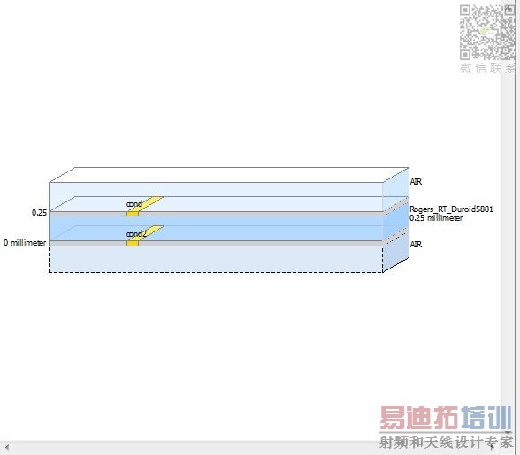
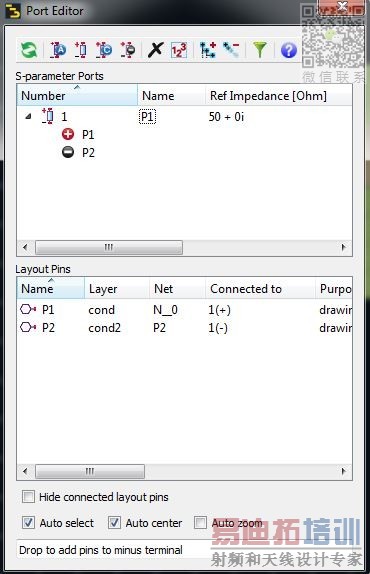
Now i want to try to simulate with finite ground plane in ADS. What I have tried up to now is to design a second patch in a different layer of cond and and connect a second port to it. Then i put the port as ground pin for port 1 from the port editor.
the problem I have is that i get warnings:
The port setup needed to be corrected:
Calibration will not be used for port "P1" (pin
sets {"P2"} and {"P1"} are in different
reference planes, although identical reference
planes are required for TML calibration).
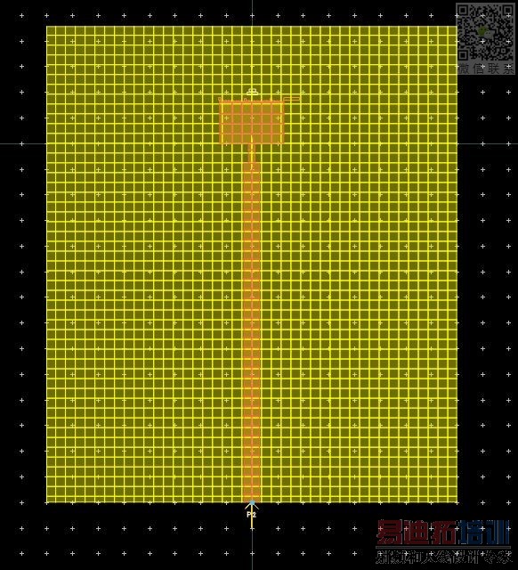
and the simulation results are very differed and is not matched anymore using the λ/4 method. Basically I thought the ground plane wont change the antenna results that much. the pictures below represents my design. Could you please tell me what I am doing wrong? or how to define a ground plate in ADS momentum.
Tas
What you shows looks correct, because there are some details to be careful about:
From the message, it seems that you have different locations (in the x-y plane) for signal and ground pin. In this case, port calibration isn't possible. By default, port calibration is "TML" and you need to switch it off.
Agilent made a strange decision when designing the ports dialog: the port calibration method is hidden, and can only be seen if you scroll right in the ports editor. So just scroll right and you will see the setting where you can change calibration from "TML" to "none".
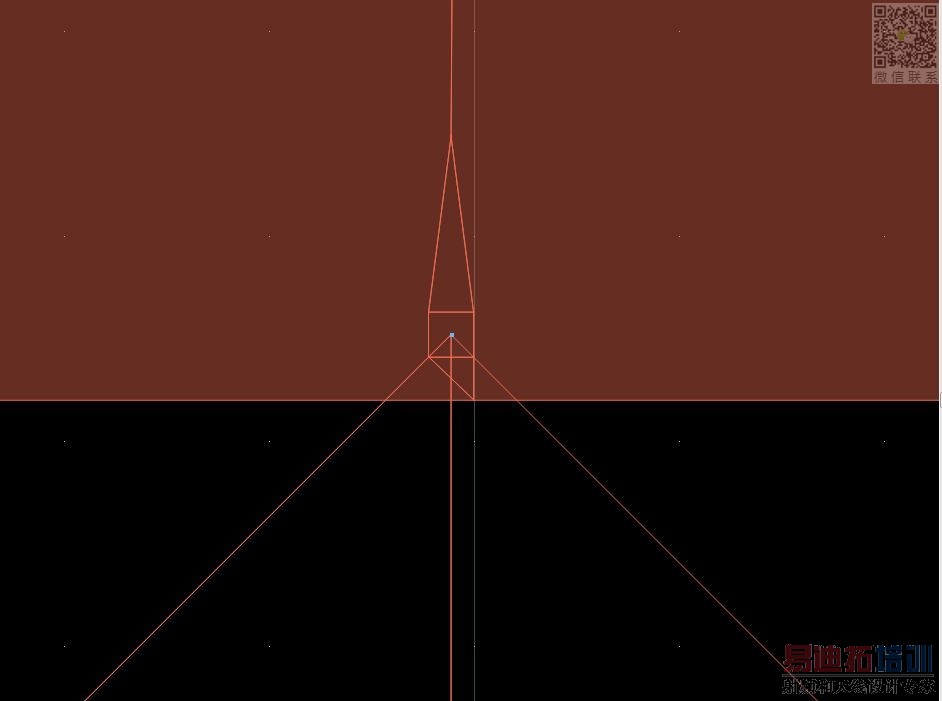
But indepedent of this warning message: do not place the pins on the edge of patch and ground plane. By default, the port would be across the entire width of the edge, and that's invalid because the edge is electrically large. Instead, you need to move the port slightly inside the polygon (to make it a point instead of an edge) or use the concept of user defined edge/area pin.
http://muehlhaus.com/support/ads-app...edge-area-pins
The ground pin must be on the ground layer at a location directly below (or very near to) the signal pin.
And yes you were right, I had the pins in different locations, I moved them in the same place and now I have better results.
I have a question tho. I am planning to use an SMA connector later on when I build the patch antenna. Most of the SMA connectors I found online have max frequency of 18 GHz. If I use them what would be the consequences?
Thanks
Tas
What is your target frequency? 24GHz?
Matching will be worse (unspecified) if you use the SMA connector above the manufacturer spec (usually 18GHz). It usually will be ok at 24GHz for hobby (amateur radio) use. If you need specified performance, use 3.5mm connectors.
http://www.microwaves101.com/encyclo...onnectors#35mm
If you go to much higher frequencies, then funny modes can propagate in the dielectric at these dimension, so higher frequency connectors use smaller dimensions.
Hi volker. Great answer
My target is 60 GHz so I am going to use 1.85 mm connector for my design. But for now..
I want to share with you my design for the single patch up to now so you understand what i am doing.
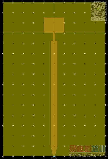
As you see in the picture I am using a simple patch, then a lamda/4 transformer, and a micro strip line to the edge of the board where the sma connector would be ( theoretical ) later on.
How long the microstrip line could be? because I cant find a way to match it to the port and the results take so long once put the ground plane :/
Thanks again
Two comments:
1. Have you looked at the middle section in my post #2 above, where I mentioned possible issue with ports on polygon edges? I can't see the port details from your screenshot.
2. Why such a long line? And why coax feed from the side with microstrip, instead of probe feed from the backside?
Yeah I ve used your advise and disable the calibration and move the pin a bit in.like this:
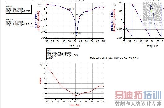
I took out the plane to optimize the patch without finite ground plane and I ll try again later.the results for s11 are ok i think. but the impedance match is not for the frequency i need from 58.5 to 61.5 GHz.
have a look.
And I dont want to use probe feed from the back direct to the board because the scale is so small.. the patch length is 1.6 mm. Most papars I found recommend the sma connector for feed. How does the length of the micro strip line affects the result? I used the LineCalc from ADS to find the width of the line for 50 Ohms.
Thanks alot for your valuable answers volker.
It is difficult to see the scale here, so we can't see what "a bit" is.
Just to avoid misunderstanding: I only suggested to switch off calibration because your previous setup (different pin locations) doesn't work with port calibration. And I only suggested to move the pin inside to avoid an electrically large port on the entire edge of the ground plane. All this was to get you started with a quick & dirty solution for finite ground plane. The accurate way to simulate with finite ground plane would be edge/area pins (my link on post #2) with port calibration enabled.
Infinite ground plane is much easier to set up, because you don't need all these extra tricks.
That's fine. Now you can move the pin on the edge of the feedline (that edge is electrically small, so this port can be across the entire edge) and enable port calibration again.
Patch antennas are narrow band. Your matching is not so very bad at the upper and lower frequency limits. But if that's not accetable, search for papers which describe methods to make them a bit more wideband.
Ok.
Longer length gives more loss. For matching, the matched 50 Ohm line will not change anything. The length calculated by linecalc is onyl relevant if you need a specific length for couplers etc.
Ok so we dont want the EM to use the whole edge of the polygon as pin. I got that part.. So how long should the line be for the edge area pin? Because I tried it on my microstrip line with width of 0.8 mm and I put a rectangle of width 0.5mm snapped to the microstrip line but I get error saying that
The port setup needed to be corrected:
Calibration will not be used for port "P1" (pin
"P1" is not on the edge between a conductive and
a nonconductive region).
Should I turn off the calibration?
thanks
Tas
Hi There. Just a quick update so there are some results for the topic.
That is my antenna design below.
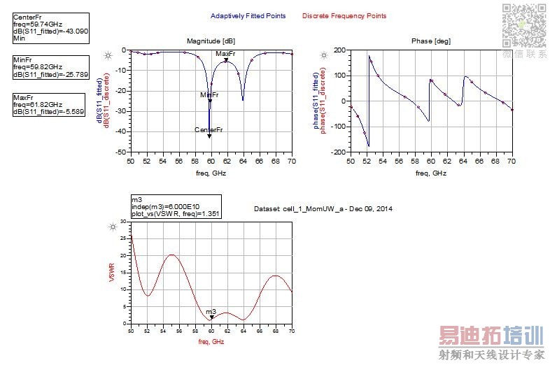
it resonates at 60 GHz gain is good but bandwidth is very small. will sort it out later.
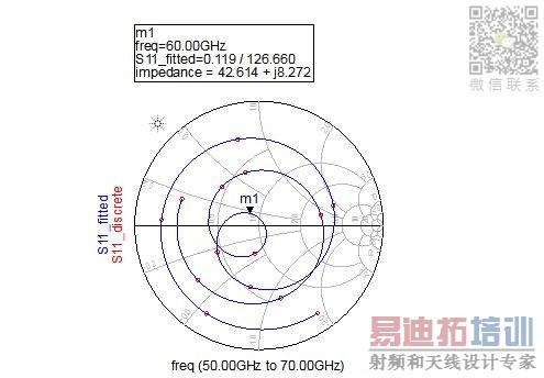
results for s11 and smith chart.
it resonates at 60 GHz and vswr is quite good.
more updates later.
Hi tasosgr54:
Have you solved the calibration problem?
Here is my design:
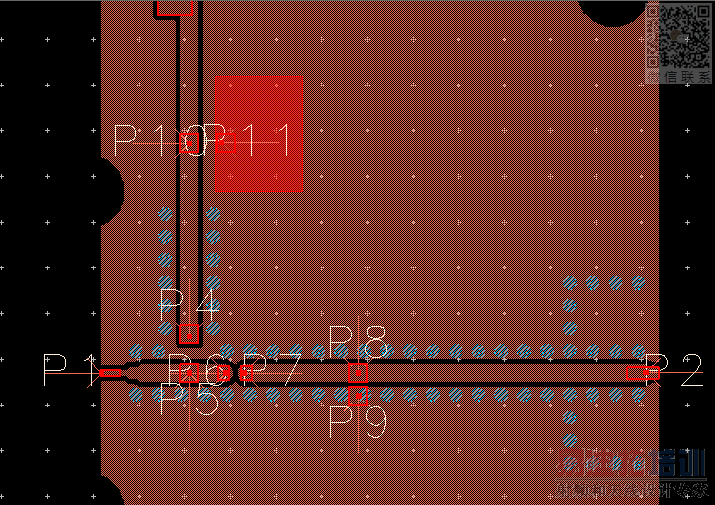
I set P1 as the area port, choosing "TML" calibration,
but encounter the same warning message:
"The port setup needed to be corrected:
Calibration will not be used for port "P1" (pin
"P1" is not on the edge between a conductive and
a nonconductive region)."
The other ports(which are all area pins) have the same warning message.
I don't know what this message mean?
I think if I choose "None" calibration there will not be these messages, but I am afraid if the result is correct.
Thanks for your reply~
申明:网友回复良莠不齐,仅供参考。如需专业帮助,请学习易迪拓培训专家讲授的ADS视频培训课程。
上一篇:Non-Integer VAR Definitions in S2PMDIF (Agilent ADS)
下一篇:port layer Definition, ADS
 国内最全面、最专业的Agilent ADS培训课程,可以帮助您从零开始,全面系统学习ADS设计应用【More..】
- Agilent ADS教学培训课程套装
- 两周学会ADS2011、ADS2013视频教程
- ADS2012、ADS2013射频电路设计详解
- ADS高低阻抗线微带滤波器设计培训教程
- ADS混频器仿真分析实例视频培训课程
- ADS Momentum电磁仿真设计视频课程
- ADS射频电路与通信系统设计高级培训
- ADS Layout和电磁仿真设计培训视频
- ADS Workspace and Simulators Training Course
- ADS Circuit Simulation Training Course
- ADS Layout and EM Simulation Training Course
- Agilent ADS 内部原版培训教材合集

