- 易迪拓培训,专注于微波、射频、天线设计工程师的培养
substrate stackup in ADS software
录入:edatop.com 点击:
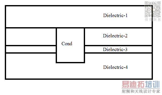
Hi! I am trying to create a substrate stackup in ADS for a 65nm technology. In the stackup I have to map a conducting material layer which passes through 3 layers of different dielectric constants. But the ADS tool does not allow the mapping of same conductor in different layers. Do you have any idea how can I solve this?
Another approach is to use "derived layers" to create clones of your via
qthelp://ads.2016.01/doc/usrguide/Adding_Derived_Layers.html
and map these new via layers separately.
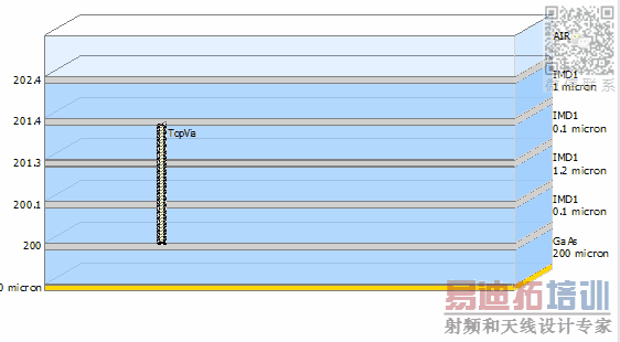
The easiest solution is to "stretch" one end of the via with the mouse, so that it goes through multiple dielectrics.
Another approach is to use "derived layers" to create clones of your via
qthelp://ads.2016.01/doc/usrguide/Adding_Derived_Layers.html
and map these new via layers separately.
The problem is that I can not make the width of the conductor bigger than the width the dielectris. For example if Conductor is 900nm wide, and Dielectric-2 is 700nm wide, I can not make Conducter's width bigger than or equal to 700nm. That is why In the next dielectric layer I have to map the same conductor to achieve a 900nm width. But this is not allowed by the ADS software. Any idea how I can do this?
You just need to split your bottom dielectric (dielectric4 in first post) into two pieces, so that you have a 200nm dielectric segment. Then, define the via to pass through dielectric2, dielectric3 and that new 200nm dielectric.
申明:网友回复良莠不齐,仅供参考。如需专业帮助,请学习易迪拓培训专家讲授的ADS视频培训课程。
上一篇:problem in ADS2003
下一篇:To design Hairpin bandpass filter using ADS
ADS培训课程推荐详情>>
 国内最全面、最专业的Agilent ADS培训课程,可以帮助您从零开始,全面系统学习ADS设计应用【More..】
- Agilent ADS教学培训课程套装
- 两周学会ADS2011、ADS2013视频教程
- ADS2012、ADS2013射频电路设计详解
- ADS高低阻抗线微带滤波器设计培训教程
- ADS混频器仿真分析实例视频培训课程
- ADS Momentum电磁仿真设计视频课程
- ADS射频电路与通信系统设计高级培训
- ADS Layout和电磁仿真设计培训视频
- ADS Workspace and Simulators Training Course
- ADS Circuit Simulation Training Course
- ADS Layout and EM Simulation Training Course
- Agilent ADS 内部原版培训教材合集