- 易迪拓培训,专注于微波、射频、天线设计工程师的培养
RF phase shifter design/optimization in ADS
录入:edatop.com 点击:
Hello everyone,
Schematic Description
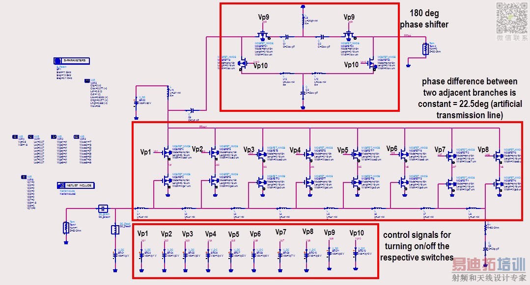
I am designing RF phase shifter in ADS at 11-12GHz for a beamformer (rf phase shifting topology). The schematic can be seen in the attached image file. As you can see, it's a combination of a 3-bit distributed phase shifter (The Cgs capacitances of the bottom nmos transistors in each branch combined whith the inductances Ls compromise an artificial transmission line with characteristic impedanse Z0=sqrt(Ls/Cgs) and constant phase shift Dph=ω*sqrt(Ls*Cgs)) and an 180 deg phase shifter.
This topology allows to vary the phase from 0deg to 360deg in steps of 22.5deg.
Question
After first design pass, the circuit is functional but it needs optimization.
When the first switch is on and all others off (Vp1=1.8, Vp2=...Vp8=0) then the phase of S21 is 0, Phase_S21_vp1=0deg.
- (Vp1=0, Vp2=1.8, Vp3=...Vp8=0) -> Phase_S21_vp1=22.5deg
- (Vp1=0=Vp2=0, Vp3=1.8, Vp4=...Vp8=0) -> Phase_S21_vp2=45deg
.
.
.
- (Vp1=...Vp7=0, Vp8=1.8) -> Phase_S21_vp8=157.5deg
How can i make this kind of sweep, where the switches are turned on sequantialy and at each step only one switch is on while all the others are off.
Also as i understand, i have to optimize 8 parameters (Phase_S21_vpi, i=1,...8.).
Any suggestions and ideas about how to set up the sweep and optimization plan in ADS would be very helpful.
Thank you in advance and sorry for long post.

I have found solution for my problem.
The way to do the kind of sweep that i asked previously is to use the BATCH SIMULATION component in ADS. More info can be found in example located in folder:
\Agilent_ADS\examples\Tutorial\BatchSim_Example1_w rk.7zap
Regards, Alex.
申明:网友回复良莠不齐,仅供参考。如需专业帮助,请学习易迪拓培训专家讲授的ADS视频培训课程。
上一篇:ADS 2016 Envelope Simulator Problem
下一篇:FinFET model for ADS
ADS培训课程推荐详情>>
 国内最全面、最专业的Agilent ADS培训课程,可以帮助您从零开始,全面系统学习ADS设计应用【More..】
- Agilent ADS教学培训课程套装
- 两周学会ADS2011、ADS2013视频教程
- ADS2012、ADS2013射频电路设计详解
- ADS高低阻抗线微带滤波器设计培训教程
- ADS混频器仿真分析实例视频培训课程
- ADS Momentum电磁仿真设计视频课程
- ADS射频电路与通信系统设计高级培训
- ADS Layout和电磁仿真设计培训视频
- ADS Workspace and Simulators Training Course
- ADS Circuit Simulation Training Course
- ADS Layout and EM Simulation Training Course
- Agilent ADS 内部原版培训教材合集
