- 易迪拓培训,专注于微波、射频、天线设计工程师的培养
RF LNA design help is needed (ADS)
Im designing a LNA using ADS.
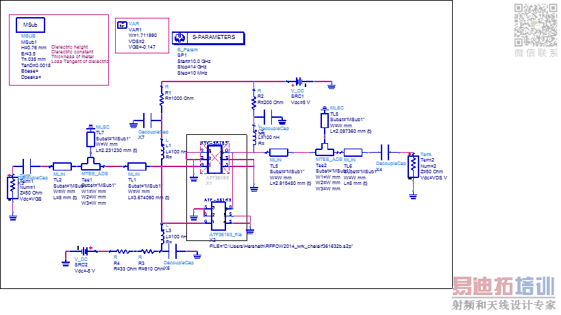
I have designed my single stub matching network and I use short circuit stubs in my design. I am getting a negative gain and I m confused about this.
If anyone can help on this it will be a great help.
What do you mean by "negative gain"? do you mean it's negative in dB, or the linear gain is negative?
yes . its negative in dB I can attach the circuit here
yes . its negative in dB I can attach the circuit here

What about the gain without matching elements? Is it above 0dB?
yes it is.
Please check your connection, do you get them right?
You made shot connected the drain and the gate by stubs...
Place DC blocking capacitors before matching circuits because short stubs make the gate and drain short circuit..
Also, the length of the shorted stubs makes no sense to me. They are very short (~2mm) and I don't think this is the correct length for impedance matching your transistors.
In this linear simulation, the bias supply doesn't have an effect, but that looks wrong. As Bigboss mentioned it is shorted to ground, and the entire configuration makes no sense (two 5V sources, R3 in series with R4, wrong gate bias voltage).
申明:网友回复良莠不齐,仅供参考。如需专业帮助,请学习易迪拓培训专家讲授的ADS视频培训课程。
上一篇:ADS power calculation in EM-Model
下一篇:ADS Layout Model Help
 国内最全面、最专业的Agilent ADS培训课程,可以帮助您从零开始,全面系统学习ADS设计应用【More..】
- Agilent ADS教学培训课程套装
- 两周学会ADS2011、ADS2013视频教程
- ADS2012、ADS2013射频电路设计详解
- ADS高低阻抗线微带滤波器设计培训教程
- ADS混频器仿真分析实例视频培训课程
- ADS Momentum电磁仿真设计视频课程
- ADS射频电路与通信系统设计高级培训
- ADS Layout和电磁仿真设计培训视频
- ADS Workspace and Simulators Training Course
- ADS Circuit Simulation Training Course
- ADS Layout and EM Simulation Training Course
- Agilent ADS 内部原版培训教材合集
