- 易迪拓培训,专注于微波、射频、天线设计工程师的培养
ADS difference between SP simulation and Transient simulation
I built a LNA at 300GHz.
so I got 21dB gain (S-Parameter simulation)
because i want to make a detector, i need a time domain graph.
but LNA didn't work.
so i sweep LNA at 50~400GHz, i got a graph attached.

why there is difference between SP sim and Tran sim ?
how i can solve this problem ?
It's possible that your circuit oscillates at around 75 GHz and in Transient simulation the circuit's performance is affected by this oscillation. Check your current and voltages and check for beginning s11 and s22 if their magnitudes become positive at around 75 GHz.
How could you get s-parameters from a transient simulation ?
I checked S22,S11
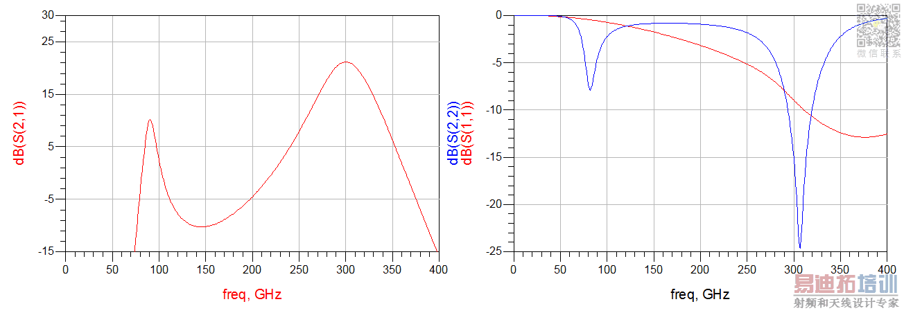
i think this circuit have not problem ..
I just checked gain from input, output peak at every 10GHz
voltage gain or power gain? S-parameter simulation is only a small-signal analysis, while transient includes large signal analysis. Nevertheless, check your current and voltage waveforms from transient analysis.
I attached some result.
i tried to HB simulation again, i got different result but i didn't change anything ..
i don't know how i solve this problem..
there are current and voltage waveforms.
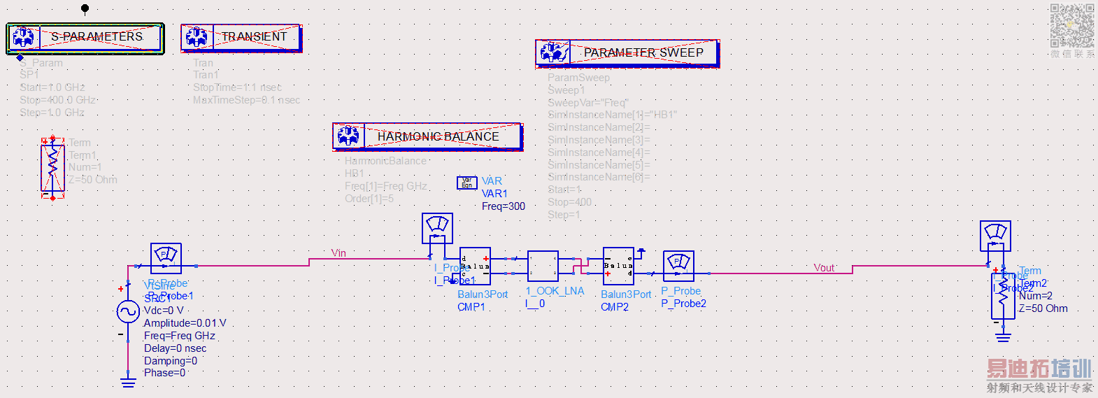
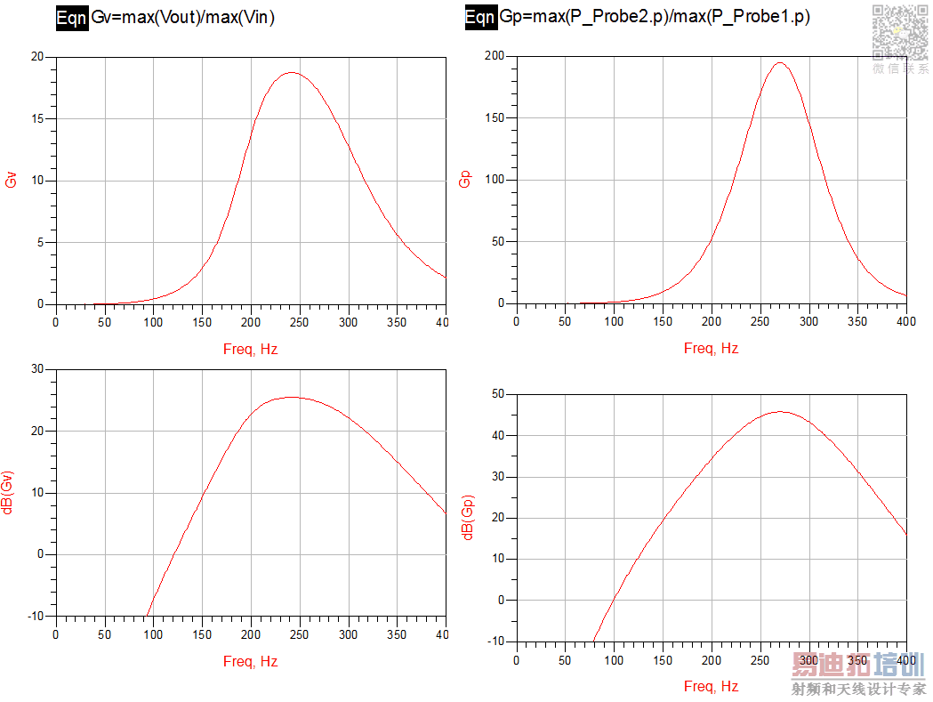
(HB result)
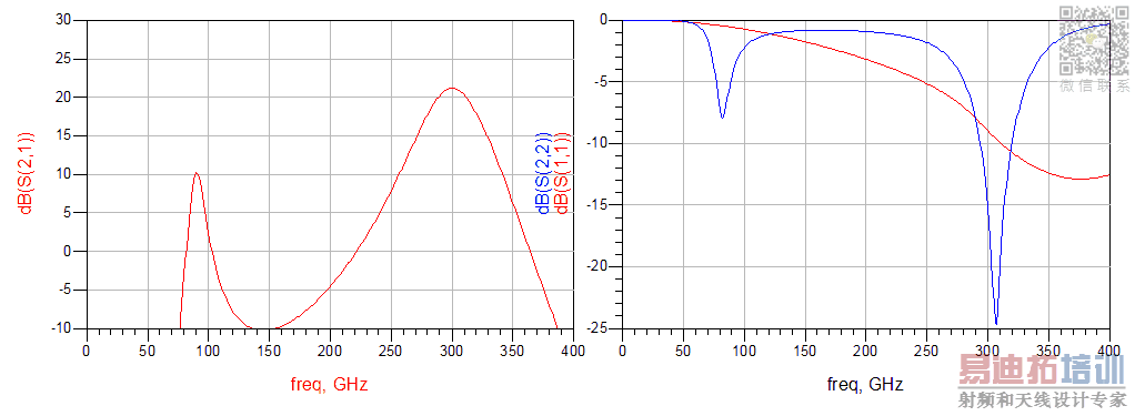
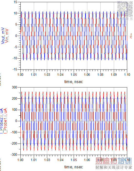
(SP and Tran result)
So for S-parameter results you take a 50 Ohm terminated source and for transient an ideal voltage source?
I revised circuit, but there is no change..


i simulate ideal BJT at TRAN and SP.
there is difference.
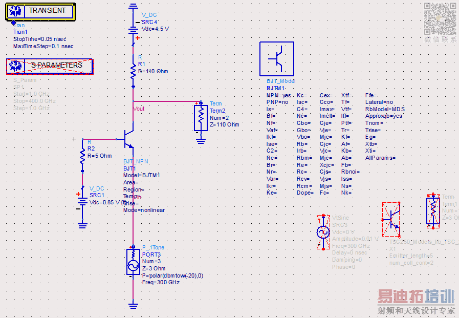
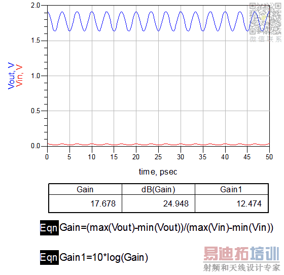
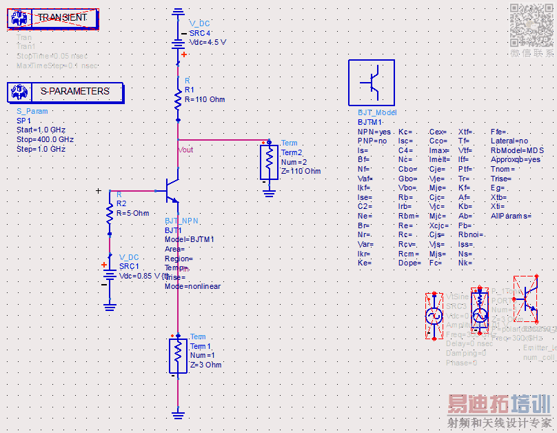
i change load's R, because matching.
why gain is different ? because SP is only small signal ?
i think active element make a difference between SP and Tran simulation.
and if i find this difference, i can solve first problem ..
Just in brief, from your first diagrams (transient ?) oscillation is visible. Second diagram, the voltage gain = 20*log (x) not 10*log (x), did you roughly calculated your voltage gain of your ideal common base ampl with gm*Rl?
By the way, for s-parameter analysis place proper dc-blocks and dc-feeds at your sources and terminals.
And last thing to remind, s21 is the forward voltage gain under matched (Zref) condition. I attached an ideal simulation with calculation of s21 and voltage gain, you see it works under matched conditions, otherwise it is not comparable.
Thank you for your help.
i have some questions.
in your circuit, load R is very large.
because check output voltage, Open circuit setting ?
my goal is check demodulator's performance.
and i need amplfying before demodulating.
if i connect amp with demodulator(input R is 50ohm) instead load, gain will be change ..
The load has a high value because of the high output impedance of the ideal transistor and to meet the matching and show the relation between s21 and voltage gain. I justed wanted to show that you can only compare s21 and voltage gain under matched condition.
Is your demodulator a real circuit? Maybe it has some additional reactive input impedance, if you connect a simple 50 Ohm resistor, its characteristic is constant over frequency and includes no reactive components.
I'm sorry very late.
I tried many things for finding difference between HB and TRAN.
I checked other components.
R, C, L show same results.
But transmission line and transistor show differences.
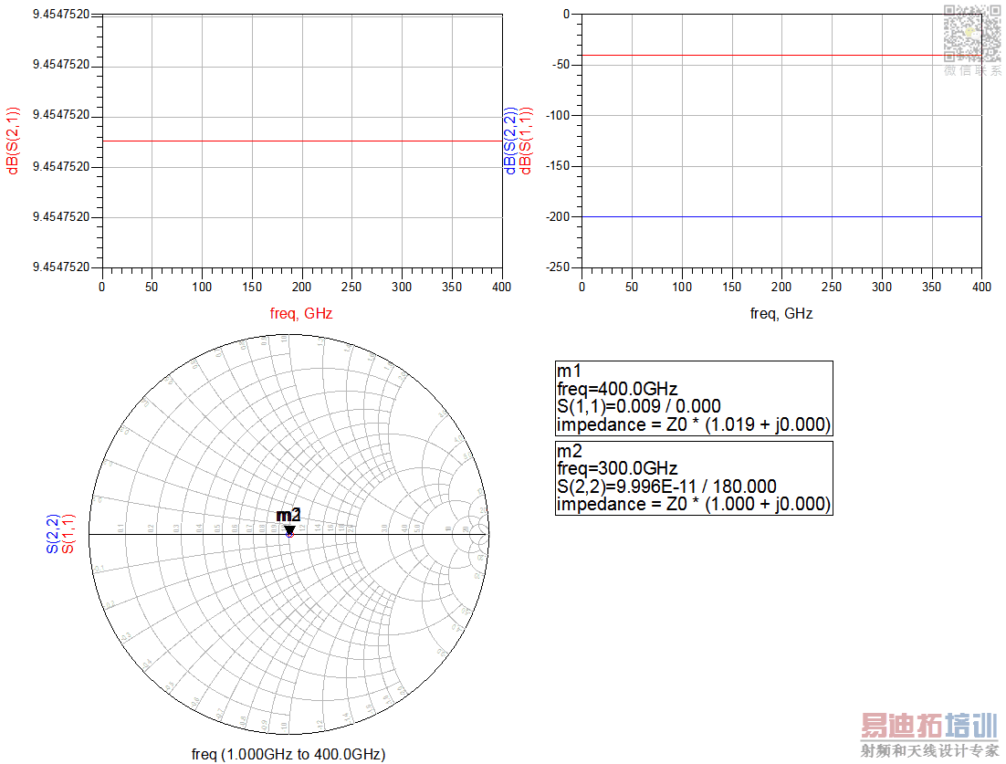
I attach results of transmission simulation.
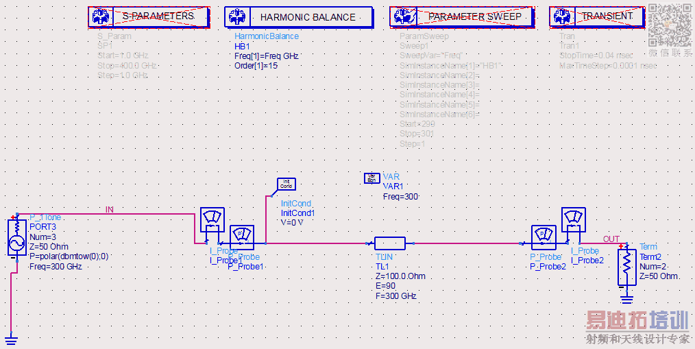
I made a very simple circuit for test.

This S21 exactly same with result of SP-Sim.
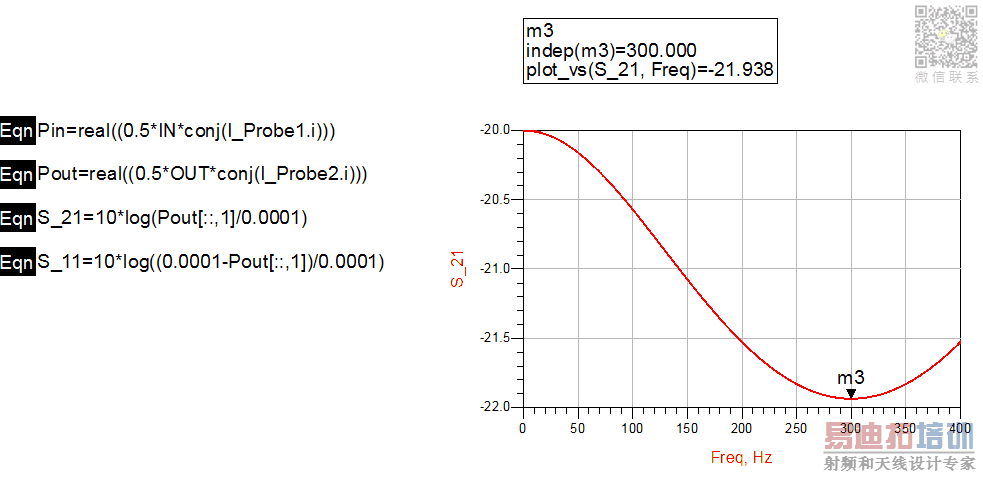

left is HB ans right is TRAN results.
I tried to deduct same Vout, Vin, Power Gain, very hard to me.
Is there some errors ? or mistakes ?
I don't know why transmission line and transistor have difference between HB and Transient.
i attach other result(change to 50ohm transmission line)

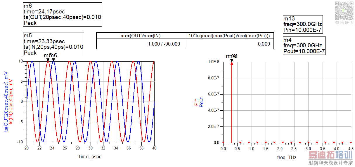
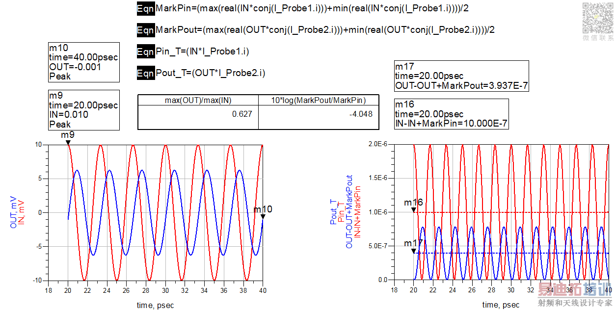
i think i miss something when simulate transient sim ..
And I find some problem.
it's okay until 250GHz.
but 250.1 GHz , it's strange
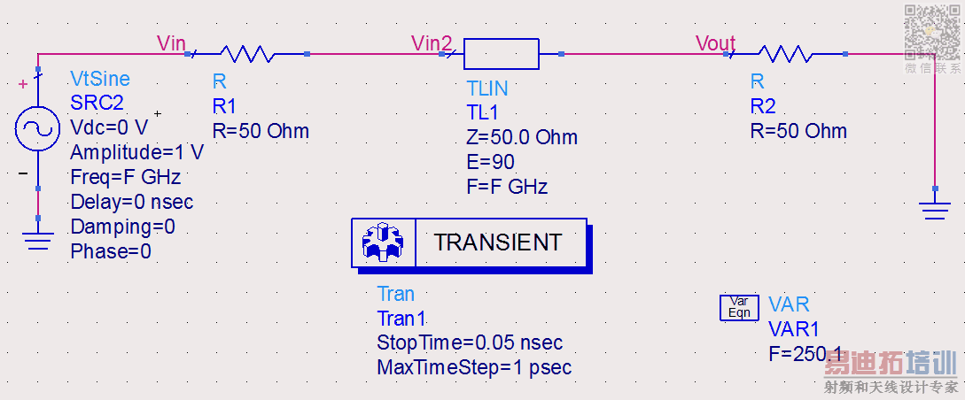
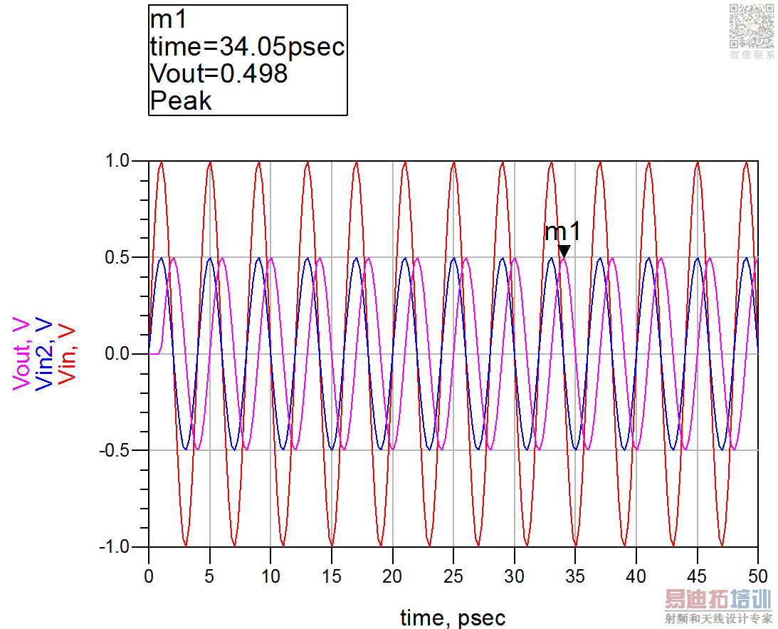
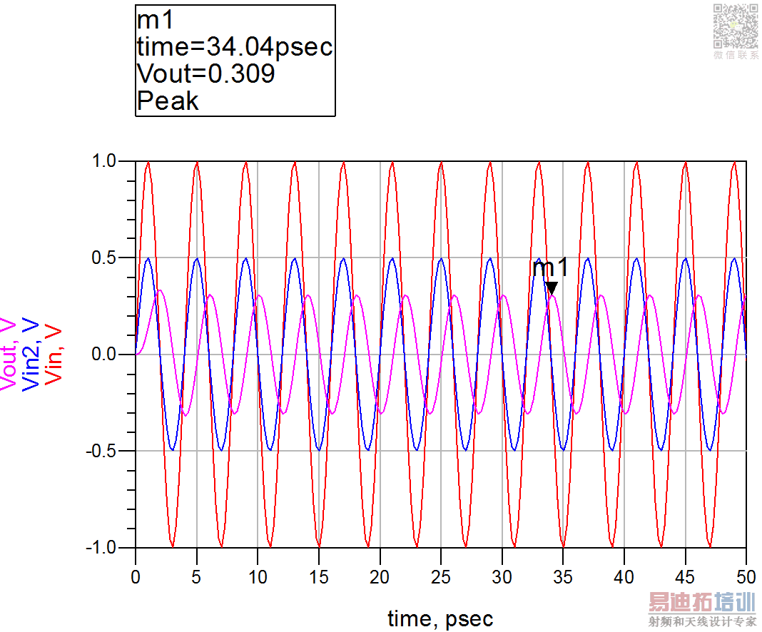
I can confirm the problem, it's the the ideal tline component, if you set F till 250 GHz, everything fine, 251 GHz you get problems. If you take instead the TLIN4 component everything works fine, also for 300 GHz. Later more.
I think TLIN4 is well.
what is difference between TLIN, TLIN4 ?
You can use a specific ground reference, that's it.
I contacted Keysight, They say ideal TLine don't have algorithm upper than 250GHz.
And they will correct this problem at next version of ADS.
Thank you for your help.
申明:网友回复良莠不齐,仅供参考。如需专业帮助,请学习易迪拓培训专家讲授的ADS视频培训课程。
上一篇:Eagle PCB Design import to ADS
下一篇:Error in creating symbol's layout (packaging) in ADS
 国内最全面、最专业的Agilent ADS培训课程,可以帮助您从零开始,全面系统学习ADS设计应用【More..】
- Agilent ADS教学培训课程套装
- 两周学会ADS2011、ADS2013视频教程
- ADS2012、ADS2013射频电路设计详解
- ADS高低阻抗线微带滤波器设计培训教程
- ADS混频器仿真分析实例视频培训课程
- ADS Momentum电磁仿真设计视频课程
- ADS射频电路与通信系统设计高级培训
- ADS Layout和电磁仿真设计培训视频
- ADS Workspace and Simulators Training Course
- ADS Circuit Simulation Training Course
- ADS Layout and EM Simulation Training Course
- Agilent ADS 内部原版培训教材合集
