- 易迪拓培训,专注于微波、射频、天线设计工程师的培养
ATF-34143 ADS model to S2P file S parameter comparison in ADS
录入:edatop.com 点击:
Hi
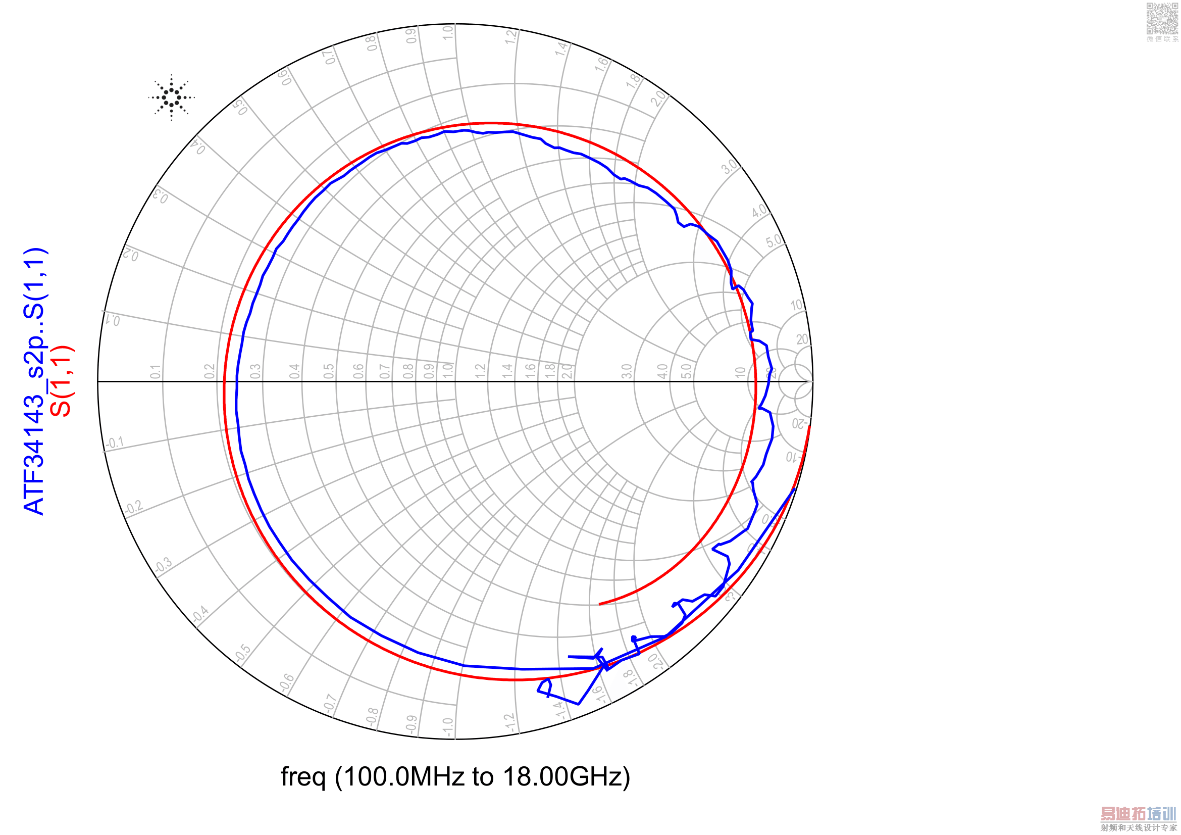
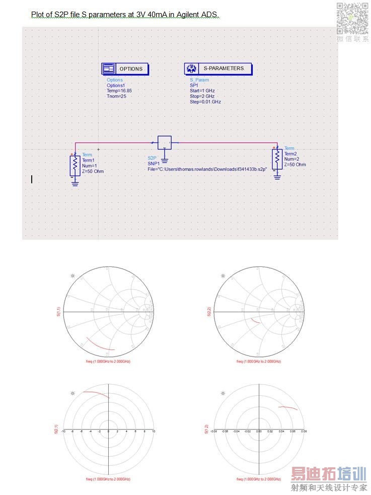
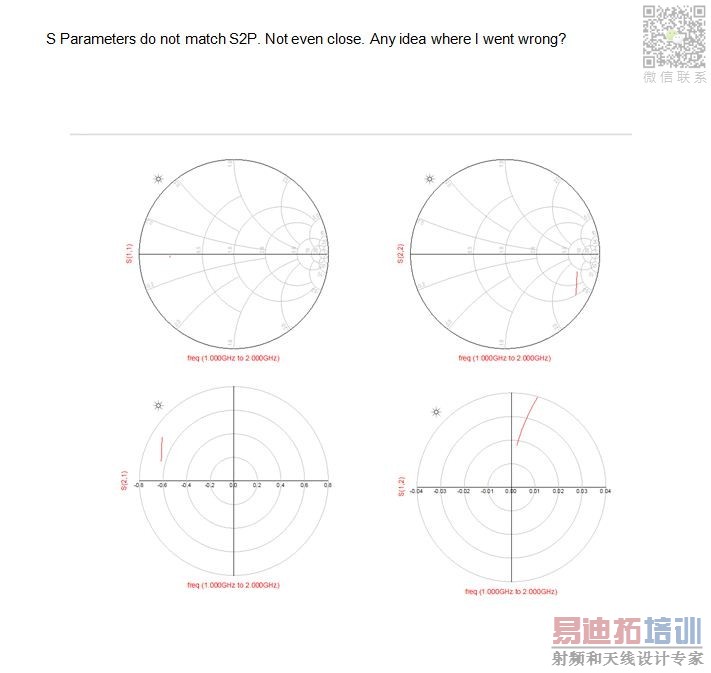
What I'm trying to do is create a bias network for avago ATF-34143 transistor model in ADS which matches the plotted S parameters of an S2P file to that of an ADS model of the transistor with a bias circuit. Bias at VDS=3 V, IDS=40 mA.
Both the model and the S2P file of the transistor are obtained from avago's website here:
http://www.avagotech.com/pages/en/rf...fet/atf-34143/
The S2P file I'm using is the f341433b.s2p - ATF-34143 s and noise parameters at 3 V, 40 mA (1 KB,S2P).
After doing this, the plots for the two simulations do not match. I have don't know why but it's probably the bias circuit I'm thinking.
I've attached some screenshots which should make things clearer.
All suggestions welcome, I am well and truely stuck. Thanks!
1-s-parameters are measured "Emitter/Source Grounded and Input and Output is terminated by 50 Ohm Characteristic Impedance"
**You used a series emitter resistance and it changes too much s-parameters.
**You have to use ideal RFC instead of Drain/Collector resistance.This R will truly change the s-parameters because it's shunted to termination impedance.
**And Gate/Base bias circuit is also not correct.You have to drive the transistor either a ideal current source for BJT or a ideal Voltage source with a RFC for FET.
What I'm trying to do is create a bias network for avago ATF-34143 transistor model in ADS which matches the plotted S parameters of an S2P file to that of an ADS model of the transistor with a bias circuit. Bias at VDS=3 V, IDS=40 mA.
Both the model and the S2P file of the transistor are obtained from avago's website here:
http://www.avagotech.com/pages/en/rf...fet/atf-34143/
The S2P file I'm using is the f341433b.s2p - ATF-34143 s and noise parameters at 3 V, 40 mA (1 KB,S2P).
After doing this, the plots for the two simulations do not match. I have don't know why but it's probably the bias circuit I'm thinking.
I've attached some screenshots which should make things clearer.
All suggestions welcome, I am well and truely stuck. Thanks!
The conditions are not same ...
1-s-parameters are measured "Emitter/Source Grounded and Input and Output is terminated by 50 Ohm Characteristic Impedance"
**You used a series emitter resistance and it changes too much s-parameters.
**You have to use ideal RFC instead of Drain/Collector resistance.This R will truly change the s-parameters because it's shunted to termination impedance.
**And Gate/Base bias circuit is also not correct.You have to drive the transistor either a ideal current source for BJT or a ideal Voltage source with a RFC for FET.


Makes much more sense now. Thanks so much!
申明:网友回复良莠不齐,仅供参考。如需专业帮助,请学习易迪拓培训专家讲授的ADS视频培训课程。
上一篇:How to check different temperature values for design of LNA IN ADS.
下一篇:How to include RF Transistor Vendor Kit in Advanced Designed Design(ADS)
ADS培训课程推荐详情>>
 国内最全面、最专业的Agilent ADS培训课程,可以帮助您从零开始,全面系统学习ADS设计应用【More..】
- Agilent ADS教学培训课程套装
- 两周学会ADS2011、ADS2013视频教程
- ADS2012、ADS2013射频电路设计详解
- ADS高低阻抗线微带滤波器设计培训教程
- ADS混频器仿真分析实例视频培训课程
- ADS Momentum电磁仿真设计视频课程
- ADS射频电路与通信系统设计高级培训
- ADS Layout和电磁仿真设计培训视频
- ADS Workspace and Simulators Training Course
- ADS Circuit Simulation Training Course
- ADS Layout and EM Simulation Training Course
- Agilent ADS 内部原版培训教材合集


