• 易迪拓培训,专注于微波、射频、天线设计工程师的培养
首页 > ADS > ADS FAQ > Problem With S-Parameter Biasing in Class A Amplifier using ADS
Problem With S-Parameter Biasing in Class A Amplifier using ADS

录入:edatop.com    点击:
I have a project to make a broadband amplifier for my subject. I used CREE N-Channel transistor GaN HEMT 40045F ( i downloaded it at youtube from keysight Loadpull simulation basic video ). And i decided to make a class A Amplifier. I also used a Self-biased as the configuration ( because i don't know how to make fixed bias configuration with Vds = 28 volt and Idq = 400 ma [ I've tried many times, but got fail all the time ] like on the datasheet.


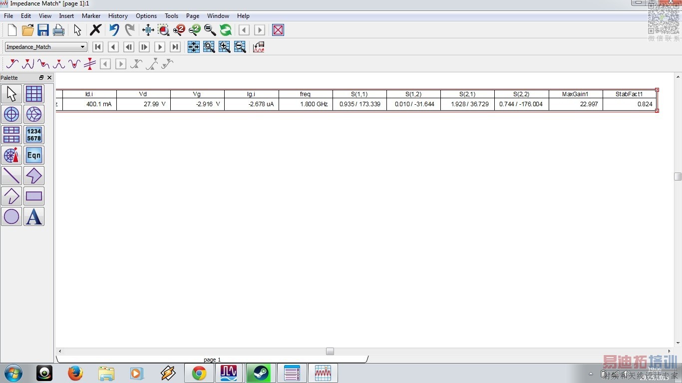
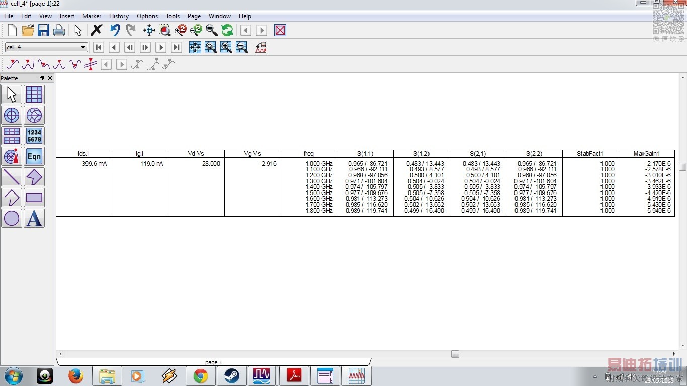
The question is, why i keep getting minus MaxGain and also the odd S-parameter ?

Thanks before

Source is floating for RF signals so s-parameters will be mistaken.

Sir, what should i do then ?
Thank you your help.

Hi,
Device should be properly matched. As you can see that your S(1,1) is almost 1. Input impedance of transistor need to be transoformed to 50 ohm.

I can see strange values from the result table you posted.

Try to:

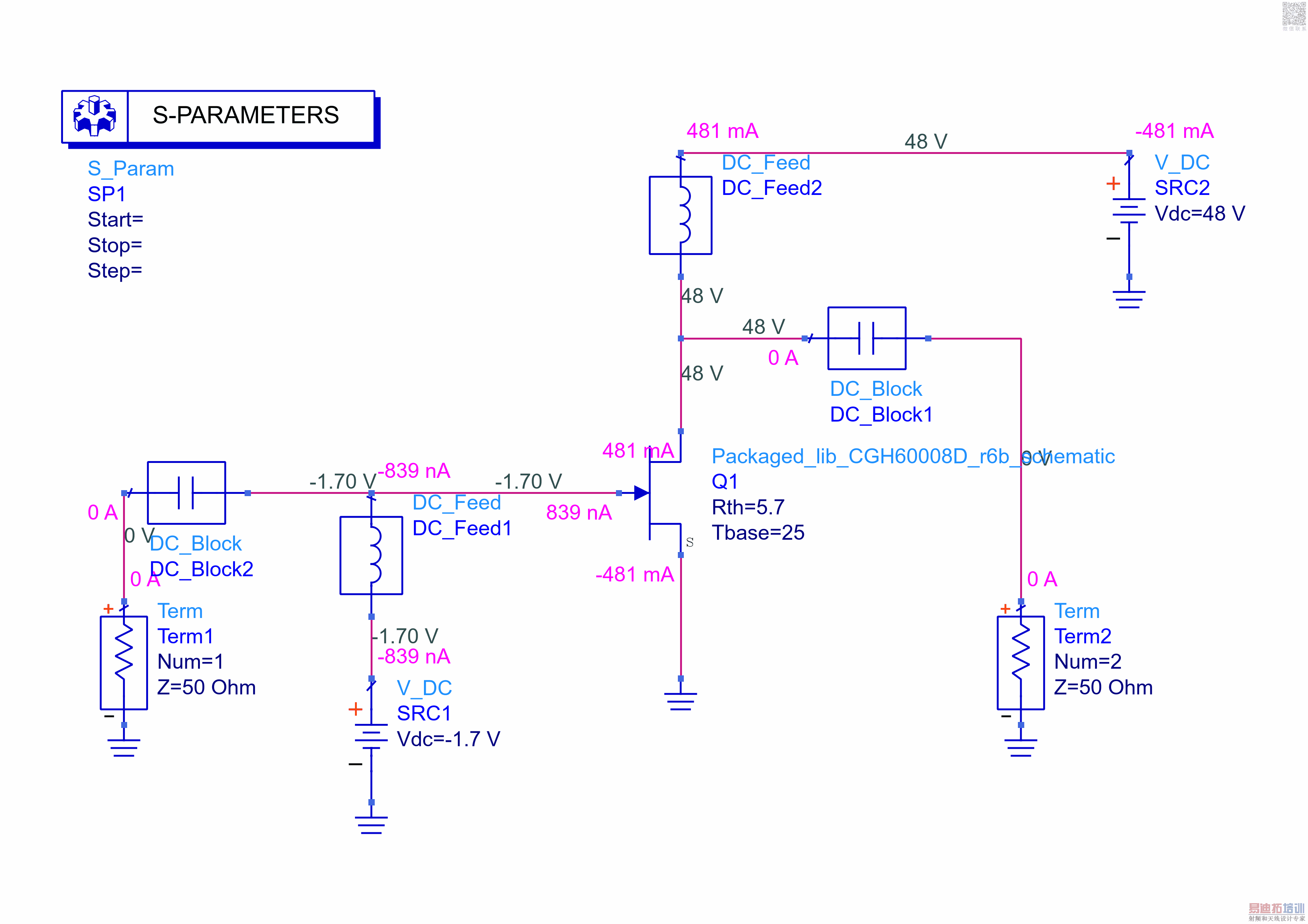
Remove DCfeed2 otherwise the RF has no return path on the transistor (as said in post #2 of BigBoss)
insert a DC voltage generator and connect it from DCfeed3 and ground (R3 can be set to 0 ohm), then reguate the voltage until you reach the operating point you want in terms of Id.

Furthermore it's better you swap Term1 with Term2, because usually Term1 is input and Term2 output, so S21 is the forward gain and S12 the reverse gain, S11 the input impedance and S22 the output impedance.

This just to start

Thank you sir for your information.

Furthermore it's better you swap Term1 with Term2, because usually Term1 is input and Term2 output, so S21 is the forward gain and S12 the reverse gain, S11 the input impedance and S22 the output impedance.

This just to start
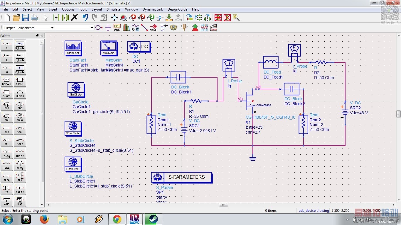
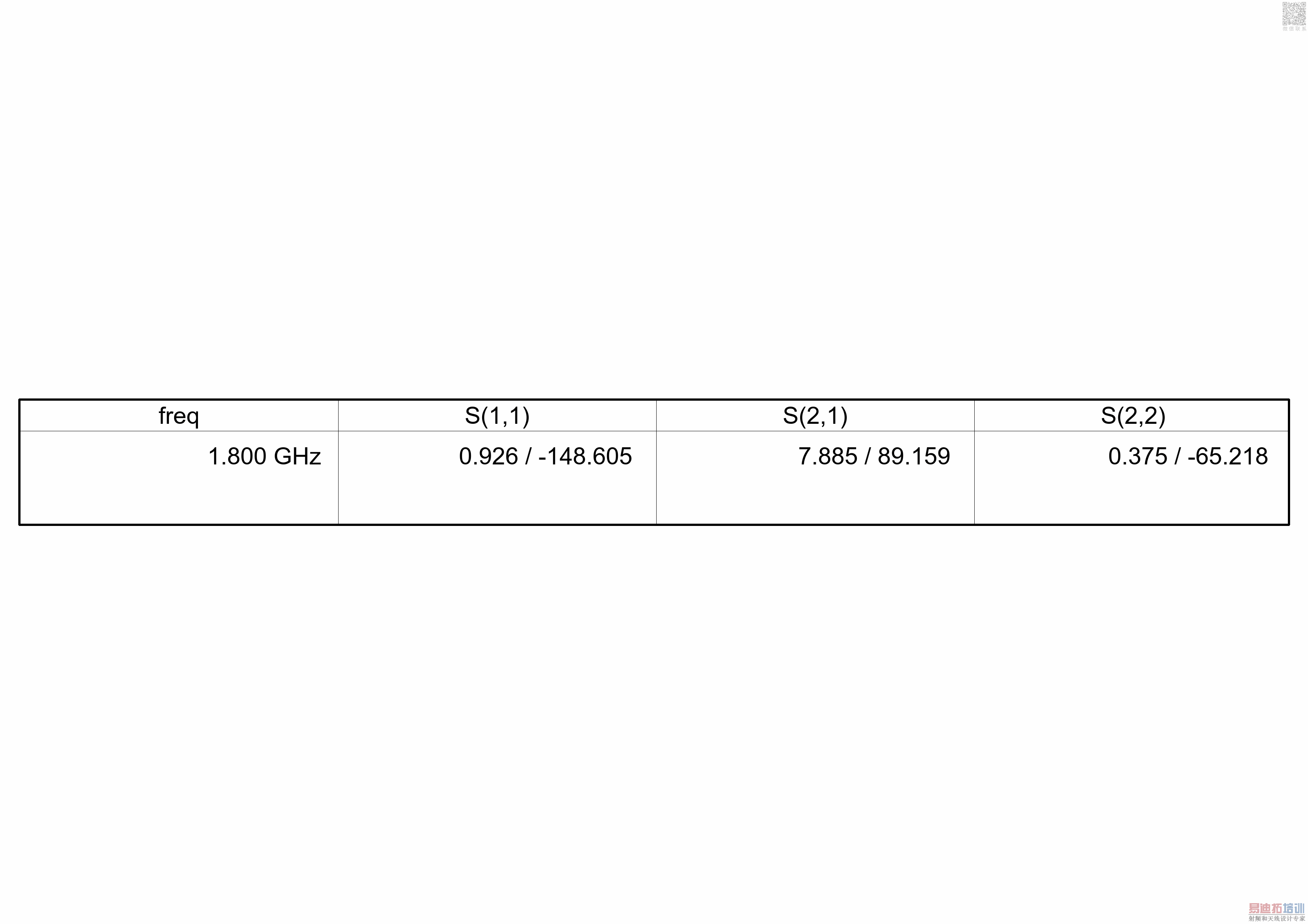
I've replaced the picture with another configuration like you've been told, and it looks nicer ( thank you ).


I want to ask sir, why DCFeed2 should be removed ( as you said that RF has no return path on the transistor, but i think about if we applied AC power from the input, DCFeed2 separate AC signal and DC signal. And if we remove the DCFeed2, the AC signal will interupt the DC signal ( i don"t know what the impact is, but i just remembered that we should separate AC signal and DC signal T___T ).

And i want to ask another question sir, when we applied biased voltage, when we want to implemented it into reality project, how can we applied -2.9161 Volt without Fixed biased configuration ( i think it's really hard to make -2.9161 power supply as the biased supply at the gate ).

Typical s-parameters simulation setup. ( You can also use template of ADS )

Thank you sir for your help.
I want to ask sir, in reality, how to make V biased ( Vdc = -1.7 v ) like you did on the picture ? Is there any external Voltage suppply that supply a voltage for about -1.7v ? Or we should calculate with biased that gives -1.7v at the gate transistor ? ( Because i found it's too hard for RF Power transistor that works at least 55 watt for the power output as the Class A amplifier configuration given below ).


Thank you.

Preferably an "external supply", e.g. an inverting DC/DC converter powered by the 28V input or an existing auxilary supply in your amplifier circuit. You need to make sure that the negative bias powers up before the drain voltage.

I think you realized that's it's no reasonable option to bias a flanged microwave transistor by a source resistor.

Sir, if i make a simple calculation, Vg= Vgs - Vs.
Vg ( which if i used a fixed bias configuration, would be [R2/R2+R1]*Vdd] )
And Vs would be Id*Rs ( i asume Id is equal to Is ).
Then if we just say that we want Vgs become -1.7, then -1.7v= Vg + Vs ( we should think that if we add Vg with Vs, the result should be -1.7v ).

And that made me confuse sir, because a source resistor would have been a 'part' also in biasing ( based on the calculation Vgs= Vg + Vs ).

I've never used a GaN HEMT as an amplifier before, i normally used BJT transistor and worked in low power and low frequency, so that the biased voltage would depend also on the emitter resistance ( source in BJT ) [ Vbase=Vbe+Vemitter ].

And my second question sir, why would we use DC/DC converter that supply a negative bias ( e.g. cuk converter with buck regulator ), why don't we use just a normal fixed bias configuration that gives -1.7V rather than use a converter DC/DC ?
I just wondered.

Thank you very much for your help sir,i really appreciate.

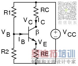
( I'm sorry if i looked too big headed, because when i learned about analog device, my lecturer said that if we want to bias a class A amplifier using BJT or FET, the best and the 'normal'
way is using Fixed bias as the configuration like the pictures below ).

申明:网友回复良莠不齐,仅供参考。如需专业帮助,请学习易迪拓培训专家讲授的ADS视频培训课程

上一篇:SMS7630 Series modeling for small signal in ADS
下一篇:ADS and axial report

ADS培训课程推荐详情>>
Agilent ADS 栏目
频道总排行

  网站地图