- 易迪拓培训,专注于微波、射频、天线设计工程师的培养
Problem with bounding area layer in ADS2011
录入:edatop.com 点击:
Hi!
I designed a simple delay line with dielectric strips in upper layer.
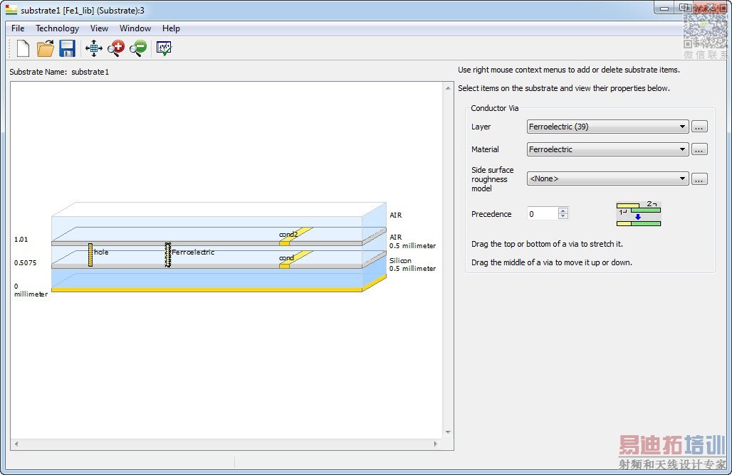
I have next problem. Bounding layer not limit dielectric area. Dielectric is everywhere.
I partially solved this problem by transfer polygons in "dielectric via layer". But this structure can't be solved with help of momentum, only with FEM.
I designed a simple delay line with dielectric strips in upper layer.
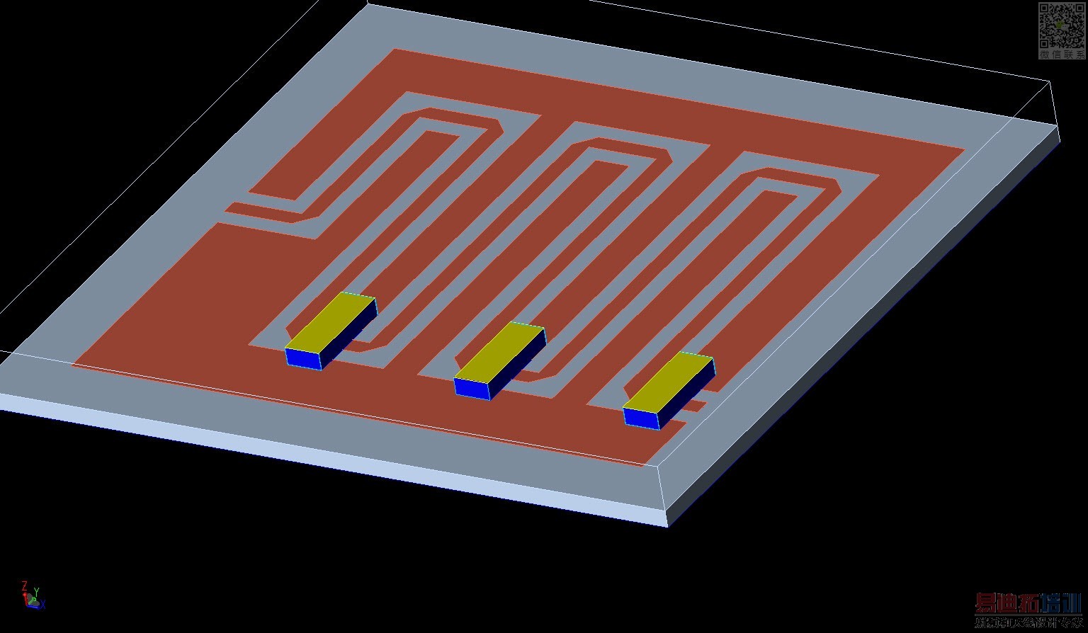
I have next problem. Bounding layer not limit dielectric area. Dielectric is everywhere.
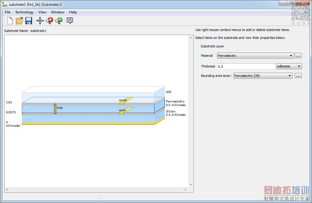
I partially solved this problem by transfer polygons in "dielectric via layer". But this structure can't be solved with help of momentum, only with FEM.
Maybe try ADS2012?
well, u built a huge 500 MHz resonator there bud. Try adding around 400 via holes from top to bottom ground layers.
Use Momentum Box.It will cover your whole structure by a closed Perfect Conductor.
For more information, read relevant help topics.
申明:网友回复良莠不齐,仅供参考。如需专业帮助,请学习易迪拓培训专家讲授的ADS视频培训课程。
上一篇:Help to solve the two detected errors in ADS2009.
下一篇:how to open s3p fle schemtic in ADS agilent
ADS培训课程推荐详情>>
 国内最全面、最专业的Agilent ADS培训课程,可以帮助您从零开始,全面系统学习ADS设计应用【More..】
- Agilent ADS教学培训课程套装
- 两周学会ADS2011、ADS2013视频教程
- ADS2012、ADS2013射频电路设计详解
- ADS高低阻抗线微带滤波器设计培训教程
- ADS混频器仿真分析实例视频培训课程
- ADS Momentum电磁仿真设计视频课程
- ADS射频电路与通信系统设计高级培训
- ADS Layout和电磁仿真设计培训视频
- ADS Workspace and Simulators Training Course
- ADS Circuit Simulation Training Course
- ADS Layout and EM Simulation Training Course
- Agilent ADS 内部原版培训教材合集