- 易迪拓培训,专注于微波、射频、天线设计工程师的培养
oscillaror simulation with ADS
录入:edatop.com 点击:
hi to all
I have a problem in simulation of my project.
these links are 2 oscillator circuits.I want simulate with ads and compare them PHASE NOISE. but those don"t have oscillate.
why?
please help me...
- - - Updated - - -
these circuits are also oscillator.can anyone simulate these with ADS and email files to me?
i'm very thankful...
my email adress is: shaban_sadeghi@yahoo.com
I have a problem in simulation of my project.
these links are 2 oscillator circuits.I want simulate with ads and compare them PHASE NOISE. but those don"t have oscillate.
why?
please help me...
What did you use for the transistor ?
There are some strange points in the second schematic.VBE of T2 is 5V ...
hi,thanks for reply.
any transistor that have noise model can be used.
i choosed a transistor such as pb_phl_BFR92A_19921214 in ADS's library.
does have oscillate circuit1?my answer is damping and no oscillating.why is damping?
I don't know from where you took those circuits, but they are not oscillators. There is no feedback network to make them oscillate. In this configuration they are just amplifiers.
thanks for reply.
but my proffesor has belief that these are oscillator.he tell first sircuit is without feedback and second is with feedback.
he says first circuit has series-current feedback.
What kind of "professor" is this, who BELIEVE that are oscillators?
Both circuits are identical, with difference the second one use a second transistor connected in a strange configuration (with base directly DC connected to Vcc, and emitter to the ground).
Sounds a bit contradictory.
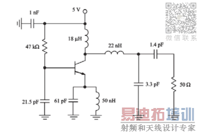
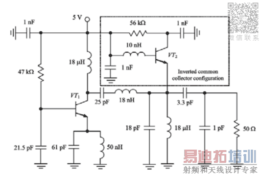
This is the text that reference these circuits:
NOISE REDUCTION TECHNIQUES
An additional active device can be used to compensate for the loss in the oscillation system.
For example, by using the inverted common collector transistor configuration, a stable negative
resistance is generated, extracting the additional energy into the resonant circuit compensating
for the loss due to the load resistance. This results in a significant increase in the loaded quality
factor of the resonant circuit. Figure 9.37 shows the schematic diagrams of the oscillators
(a) without compensation circuit and (b) with compensation circuit [37]. The soft start-up and
steady-state oscillation conditions are realized by using the capacitive feedback reactance in
the base and inductive reactances in the emitter and collector circuits. Both circuits have the
same terminal impedances at the emitter and base ports, but different in the collector port.
After incorporating the negative resistance circuit based on a common collector transistor VT2,
the collector of the main transistor VT1 sees the inductive impedance with the resistive part
approaching zero. At oscillation frequency of 800 MHz with output power of -6.8 dBm, the
oscillator with compensation negative resistance circuit provides 6 dB phase noise improvement
at 10 kHz offset.
Also I was able to run the first circuit using a BFP420 transistor in Ansoft Designer, but I had to increase the values of the matching circuit on the output. I doubled the three values. With the standard values it wanted to oscillate around 1.5Ghz
It simulates with a fundamental of around 880Mhz with level close to 0dBm.
sorry LVW
first circuit has feedback and it is series_current.and second don't have feedback.
my professor is very skillful and i don't think that he say false.can you simulate these circuits with ADS?
my friend reach to sin waveform at second circuit and at first i have problem...
- - - Updated - - -
thank you very much E-design.
your reply is helpful.can you halp me in first circuit?my answer is damping,when simulate it with ADS software.
I put the first circuit in ADS and MWO and doesn't oscillate at all, using BFP420 and any combination of matching output network (different values).
For me make sense, there is minimal feedback in this circuit using the original components, which actually this was the original question of the post. Of course, if start playing with values and add components it will oscillate at some point.
Second circuit is a bluff. The DC current through VT2 is 1 Amp, which will kill the transistor in the first millisecond.
hi vfno.you say these circuits doesn't work?E-design say true.circut 2 is used for compensate of path loss.but my simulation in ADS doesn't oscillate.I don't know why.do you simulate these circuts with harmonic balance in ADS?can you email for me your simulations?my email is: shaban_sadeghi@yahoo.com.
thanks alot...
I agree with vfone about the last circuit. There must be a drawing error with the last circuit. As drawn the VT2 transistor will fail. If anyone can get hold of the paper "Electronic Letters, issue 29, pg 379 - 381" it should clear up the correct configuration of the VT2 circuit.
I checked circuit 1 in Ansoft as well as MWO and the results sort of agree. Phase noise is not good at all. Without knowing what transistors the author used in his examples it would be difficult to evaluate properly. As soon as I can get access to a ADS platform, I will attempt to get a simulation result.
[37] V. M. T. Lam and P. C. L. Yip, ?Microwave Oscillator Phase Noise Reduction Using Negative
Resistance Compensation?, Electronics Lett., 29, 379?381 (1993).
The MWO simulation used the non-linear model provided by Modelithics, and for Ansoft, the internal non-linear model by Infineon was used.
This circuit was featured in High Frequency Electronics in July 2005 as a multi part series on osc design by Andrei Grebennikov
These circuits are straight out of this High Frequency Electronic article "Noise Reduction in Transistor Oscillators: Part 3", Fig 35
hi E-design.
transistor that author used is NEC2sc3358 BJT.why this circuits don't have steady soscillation?
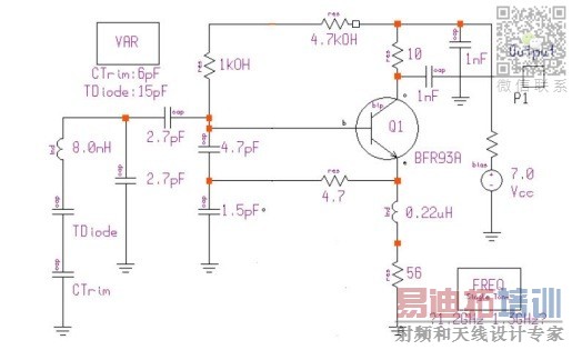
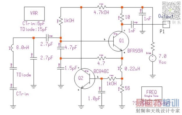
my friends...what is your idea about following circuits?
- - - Updated - - -
these circuits are also oscillator.can anyone simulate these with ADS and email files to me?
i'm very thankful...
my email adress is: shaban_sadeghi@yahoo.com
Here are the results with MWO of your last two circuits.
I have done some simulations on these circuits using ADS a few years ago. I will try to find the files for you.
Ok, I found some results of that ADS simulation that I documented Still looking for the actual project files.
hi E-design.these are different a little,but are useful.thanks for your attention.i could simulate first circuit as you say.but i want simulate these with original values.this simulation be comlicated
what do you mean?
namely,when i simulate these circuits with ADS,i don't know don't simulate.main problem is simulate these circuits with initial values of elements in circuits.i don't want change their values...
Well, you won't be able to simulate the 2nd circuit as shown at the start of this thread. There is some error in the circuit of the negative resistance generator formed by VT2. Point this out to your Professor. You should be able to simulate the last set of circuits using ADS by using the same controllers, and set up as shown in my circuit diagram.
hi E-design.how are you?i showed the circuit with negative resistance to my proffesor and he has opinion that this circuit will oscillate.
can you tell me that what transistor you used in your design of last set of circuits with ads?transistor names are not specified...because each transistor change oscillation conditions...
申明:网友回复良莠不齐,仅供参考。如需专业帮助,请学习易迪拓培训专家讲授的ADS视频培训课程。
上一篇:compatability of ADS 2011.10
下一篇:efficiency equation in ADS
ADS培训课程推荐详情>>
 国内最全面、最专业的Agilent ADS培训课程,可以帮助您从零开始,全面系统学习ADS设计应用【More..】
- Agilent ADS教学培训课程套装
- 两周学会ADS2011、ADS2013视频教程
- ADS2012、ADS2013射频电路设计详解
- ADS高低阻抗线微带滤波器设计培训教程
- ADS混频器仿真分析实例视频培训课程
- ADS Momentum电磁仿真设计视频课程
- ADS射频电路与通信系统设计高级培训
- ADS Layout和电磁仿真设计培训视频
- ADS Workspace and Simulators Training Course
- ADS Circuit Simulation Training Course
- ADS Layout and EM Simulation Training Course
- Agilent ADS 内部原版培训教材合集