- 易迪拓培训,专注于微波、射频、天线设计工程师的培养
Wide microstrip line ADS simulation - PA output matching network help
录入:edatop.com 点击:
Hi.
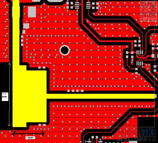
I am trying to simulate output matching network of PA. As a first step i am simulating S21 of OMN without lumped elements: only microstrip lines. I have some wide lines at OMN (up to 21mm width). I know that ADS models isn't accurate for such case so i use Momentum. But results that i received is not even close to what i measured using network (i am simulating existing PA, trying to improve it).
For a while whole simulation at momentum.
Can anybody help me with some hint, may be i missing something?
Thanks a lot
At the transistor end, include a very short segment of transmission line with the width of your transistors leads. This is important to miodel the step in width between transistor lead and the wide patch.
I know, but you can't use the step for such wide lines - those the reason why i use momentum. Any way at the first step i refer my simulation to measured OMN without transistor. Step is not an issue here, but thanks
I understand that you use Momentum, and I have some experience with troubleshooting this exact case in EM modelling ...
The problem is the width of the port at the transistor end. You must make sure that Momentum port width = terminal width of the transistor. The step in width causes inductance and is an important part of the matching network.
Well, i understood and i'll try it at the evening, thanks.
But when i measure the OMN with network i soldered the small calibrated coax to OMN input: without transistor lead step issue at all - it is my reference for simulation.
... and this creates a big step in width between the coax center connector and the wide patch. But if you place the Momentum port at the wide patch, without adding a step, the port will have a width of 21mm. This very different.
Unfortunately, it didn't help. I'll simulate it using CST only to check myself but additional suggestions\help are welcomed
If you want to upload the layout (DXF or ADS zap file), I can give it a try in Sonnet EM as well.
Thanks a lot
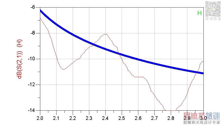
Can you show your measured result compared to the simulated ones?
Blue is simulation results. I got the same with CST when use an open boundaries so i gonna measure my pcb another time.
I started to look at your ADS model, and noticed that the vias in the ground planes are missing. I will re-simulate in Sonnet with and without vias, and post results later today.
- - - Updated - - -
Sonnet simulation with and without the vias to ground finished: there is no substantial difference, except for a small dip in S21 at 2.1GHz with missing vias. The simulations do not show the large, slow ripple in S21 that you have measured. It makes sense to repeat the measurement.
I know, thanks. I repeated the measurement as i intended after i got the same results using CST. I make a larger span and for lower frequencies (below 2GHz)) ) my simulation looks similar to measurement. Simply the large ripples above 2GHz confused me - probably i need to design a taper to connect to low impedance line.
Hi all. I continued my simulation concentrating on EB OMN. When i add to Momentum more ports (for further connection of capacitors after i turn it to component) my initial S21 result changed and some ports turns during simulation to internal although physically no overlapping exists.
I put all ports 50ohm may be it's an issue?
I am simulating OMN of EB of:
http://www.freescale.com/files/rf_if...MW7IC2750N.pdf
申明:网友回复良莠不齐,仅供参考。如需专业帮助,请学习易迪拓培训专家讲授的ADS视频培训课程。
上一篇:ADS simulation for switched beam smart antenna
下一篇:axial ratio using ADS
ADS培训课程推荐详情>>
 国内最全面、最专业的Agilent ADS培训课程,可以帮助您从零开始,全面系统学习ADS设计应用【More..】
- Agilent ADS教学培训课程套装
- 两周学会ADS2011、ADS2013视频教程
- ADS2012、ADS2013射频电路设计详解
- ADS高低阻抗线微带滤波器设计培训教程
- ADS混频器仿真分析实例视频培训课程
- ADS Momentum电磁仿真设计视频课程
- ADS射频电路与通信系统设计高级培训
- ADS Layout和电磁仿真设计培训视频
- ADS Workspace and Simulators Training Course
- ADS Circuit Simulation Training Course
- ADS Layout and EM Simulation Training Course
- Agilent ADS 内部原版培训教材合集