- 易迪拓培训,专注于微波、射频、天线设计工程师的培养
ADS 2009 layout multilyer question
录入:edatop.com 点击:
Hi everybody
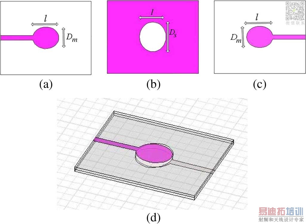
how to draw the attached structure in the ADS layout?
Thanks in advance
It is not possible to draw eliptical shapes directly. In this cas draw a circle with diameter of l and then convert it to a polygon (Edit > Modify > Convert To Polygon). Next use scaling (Edit > Scale/Oversize > Scale...) to change the height smaller to Dm or larger to Ds as required. This should create a polygon with the closest outline.
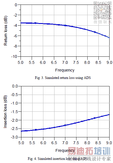
Notice that the insertion loss should be minimum, as this shows good power transfer and low losses. also S(1,1) and Phase(S(2,1)), should show UWB characteristics as it should be 30 deg phase shift from 1-2 for a wide band.
Now meaning of UWB according to FCC is 3.1 GHz to ~10.6 GHz. Also from the figure I can tell you that you have created wrong slot layer, notice that the oval shape in the diagram is perpendicular to the upper and lower patch oval shape. you can correct it and re-check the design.
-----
Amit
ADVERTISING LINK REMOVED
how to draw the attached structure in the ADS layout?
Thanks in advance
You got 3 metal layers and no GND.So you should use "stripline" configuration in substrate definition.
For big hole, you should use "boolean" property of layout editor.
Definitely what BigBoss says.
For the middle layer draw the two shapes, the outline and the inner cut-out shape and then use "Edit > Merge > Union Minus Intersection" to create the overall polygon.

It is not possible to draw eliptical shapes directly. In this cas draw a circle with diameter of l and then convert it to a polygon (Edit > Modify > Convert To Polygon). Next use scaling (Edit > Scale/Oversize > Scale...) to change the height smaller to Dm or larger to Ds as required. This should create a polygon with the closest outline.

you should define the strip-line ports also, IMHO.
I would think that the center layer is the ground in this circuit.
If we want to create the regular layout, draw the layout as RealAEL has described. But obviously, there are no circuit/schematic models to simulate this type of layout, and we need to use EM analysis.
For efficient EM analysis with Momentum, the "simulation layout" would be created differently than the "regular" layout: In Momentum, you can map the ground as a "slot" layer instead of a "strip" layer. This with mesh the slot instead of the metals, and use a "magnetic current" approach for more efficient simulation. To use this slot layer simulation, you need to draw the layout where there is NO metal. In your case, you draw the hole instead of the metal.
Top and bottom layer: map as strip layer, draw condutors
Middle ground layer: map as slot layer, draw hole
Thank you all
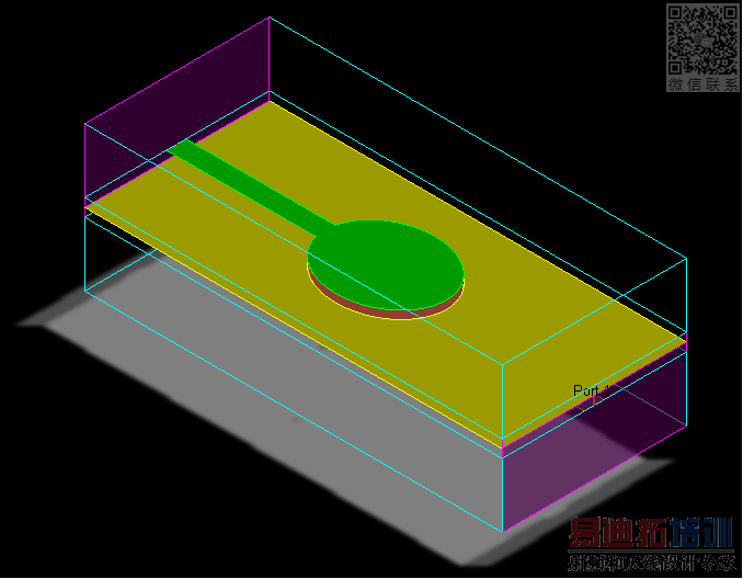
I have attached the layout drawn by myself, but didnt get the expected results ANY SUGGESTION?
Best regards
What is the exact theory behind of this idea ?
I draw as you said-I hopefully understood you well
Do you know the way how Momentum models CPW with "magnetic currents" and slot layer mapping, rather than electric current and strip layer mapping? My suggestion was to apply the same thing here. In your layout, the outer frame on the ground layer should be removed, because that layer is the INVERSE of metal and your drawn ring would correspond to a slot.
However, I am not a Momentum user myself and might have missed some difficulty in port setup for mixed strip/slot layers. So if it doesn't make sense, just go with the "normal" strip layer configuration as saeedbayanlou has already simulated.
The drawing looks like it's a capacitor, so the output file looks reasonable. What are you trying to make ?
It's an UWB 30 degree phase shifter.
Ok.
From the graphs you have I would say that if you made the circle ~ twice as big
you will get less Insertion loss and better return loss (if that's what you need).
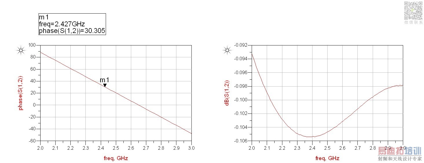
Also you should show a plot of your phase. You may have a good design for shifting
30° over your desired bandwidth.
Hi saeedbayanlou,
If its a 30 deg phase shifter, then the S parameters results should be like
Notice that the insertion loss should be minimum, as this shows good power transfer and low losses. also S(1,1) and Phase(S(2,1)), should show UWB characteristics as it should be 30 deg phase shift from 1-2 for a wide band.
Now meaning of UWB according to FCC is 3.1 GHz to ~10.6 GHz. Also from the figure I can tell you that you have created wrong slot layer, notice that the oval shape in the diagram is perpendicular to the upper and lower patch oval shape. you can correct it and re-check the design.
-----
Amit
ADVERTISING LINK REMOVED
申明:网友回复良莠不齐,仅供参考。如需专业帮助,请学习易迪拓培训专家讲授的ADS视频培训课程。
上一篇:alim coax with agilent ADS
下一篇:ADS - Finding Derivatives
ADS培训课程推荐详情>>
 国内最全面、最专业的Agilent ADS培训课程,可以帮助您从零开始,全面系统学习ADS设计应用【More..】
- Agilent ADS教学培训课程套装
- 两周学会ADS2011、ADS2013视频教程
- ADS2012、ADS2013射频电路设计详解
- ADS高低阻抗线微带滤波器设计培训教程
- ADS混频器仿真分析实例视频培训课程
- ADS Momentum电磁仿真设计视频课程
- ADS射频电路与通信系统设计高级培训
- ADS Layout和电磁仿真设计培训视频
- ADS Workspace and Simulators Training Course
- ADS Circuit Simulation Training Course
- ADS Layout and EM Simulation Training Course
- Agilent ADS 内部原版培训教材合集