- 易迪拓培训,专注于微波、射频、天线设计工程师的培养
steps check for multi-layer quadrature coupler in hfss and ads
录入:edatop.com 点击:
Hi,
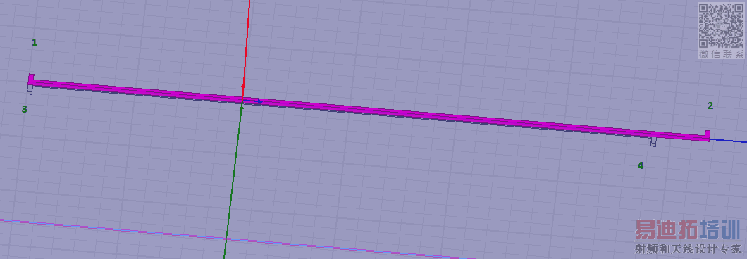
I have designed a multi-layer quadrature hybrid coupler(can be offset) in HFSS and assigned 4 ports to it as shown:
Port 1: input
Port 2: transmitted
Port 3: coupled
Port 4: isolated
Step 1: I designed each layer to be a quarter wavelength at the frequency of my interest. Such that Length_1 (top metal layer) = X um. Length_2 (the next metal layer) = Y um
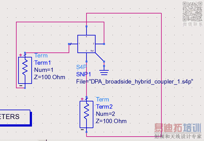
Step 2: Simulate the 4 ports and then port the s4p file to ADS for simulation
Step 3: Connection is as seen:
Questions:
1) Why can't i connect 1&4, 2&3 in a differential way? (results will be very wrong with k value more than 1). Because usually you'll see port 1,4 on the left side and port 2,3 on the right side (Edit: this is a stupid comment to give am sorry. Could it be because ports 1 and 2 are on the same layer and vice versa for 3 and 4?)
2) Upon configuring as shown, I can use the Z parameters to obtain the Zeven and Zodd to get the values that I want?
3) In HFSS, i should trial and error W1 and W2 for the respective metals and the offset (the overlap length from the cross sectional view) to give me the broadband 90 degree that I want at the range of frequency of my interest?
Any help would be appreciated or even pointing out what I've done wrongly here. Thanks!
Natnoraa
I have designed a multi-layer quadrature hybrid coupler(can be offset) in HFSS and assigned 4 ports to it as shown:

Port 1: input
Port 2: transmitted
Port 3: coupled
Port 4: isolated
Step 1: I designed each layer to be a quarter wavelength at the frequency of my interest. Such that Length_1 (top metal layer) = X um. Length_2 (the next metal layer) = Y um
Step 2: Simulate the 4 ports and then port the s4p file to ADS for simulation
Step 3: Connection is as seen:

Questions:
1) Why can't i connect 1&4, 2&3 in a differential way? (results will be very wrong with k value more than 1). Because usually you'll see port 1,4 on the left side and port 2,3 on the right side (Edit: this is a stupid comment to give am sorry. Could it be because ports 1 and 2 are on the same layer and vice versa for 3 and 4?)
2) Upon configuring as shown, I can use the Z parameters to obtain the Zeven and Zodd to get the values that I want?
3) In HFSS, i should trial and error W1 and W2 for the respective metals and the offset (the overlap length from the cross sectional view) to give me the broadband 90 degree that I want at the range of frequency of my interest?
Any help would be appreciated or even pointing out what I've done wrongly here. Thanks!
Natnoraa
1) Solved. I must go back to HFSS and found that port 3 is actually the transmitted port looking at the phase S31. it leads S21 by about 90 degree and thus port 2 should be the coupled port. By connecting port 1,3 and 2,4 one can get the correct differential results
2) Solved.
3) Solved. Got a phase imbalance of about 4 degrees in the frequency range of interest. not the best but should be okay.
Thanks for viewing
Natnoraa
申明:网友回复良莠不齐,仅供参考。如需专业帮助,请学习易迪拓培训专家讲授的ADS视频培训课程。
上一篇:re: need help in mixer design bu ADS
下一篇:ADS design of a positive feedback oscillator ( 10,6Ghz ) Urgent
ADS培训课程推荐详情>>
 国内最全面、最专业的Agilent ADS培训课程,可以帮助您从零开始,全面系统学习ADS设计应用【More..】
- Agilent ADS教学培训课程套装
- 两周学会ADS2011、ADS2013视频教程
- ADS2012、ADS2013射频电路设计详解
- ADS高低阻抗线微带滤波器设计培训教程
- ADS混频器仿真分析实例视频培训课程
- ADS Momentum电磁仿真设计视频课程
- ADS射频电路与通信系统设计高级培训
- ADS Layout和电磁仿真设计培训视频
- ADS Workspace and Simulators Training Course
- ADS Circuit Simulation Training Course
- ADS Layout and EM Simulation Training Course
- Agilent ADS 内部原版培训教材合集
