- 易迪拓培训,专注于微波、射频、天线设计工程师的培养
How to simulate in ADS layout using ground polygon?
录入:edatop.com 点击:
Hello all.
Anybody knows how to simulate in a ADS layout with using ground polygon. I want to add the ground polygon.. how could i do it? Please help i have to simulate misrostiplines with nearby ground polygon.
Anybody knows how to simulate in a ADS layout with using ground polygon. I want to add the ground polygon.. how could i do it? Please help i have to simulate misrostiplines with nearby ground polygon.
To do simulate proximity effects of groundplane close to microstrip lines within ADS you would need to use EM simulation with Momentum (planar EM) or EMDS (3D EM). Regular circuit simultor models will not be able to characterize these effects.
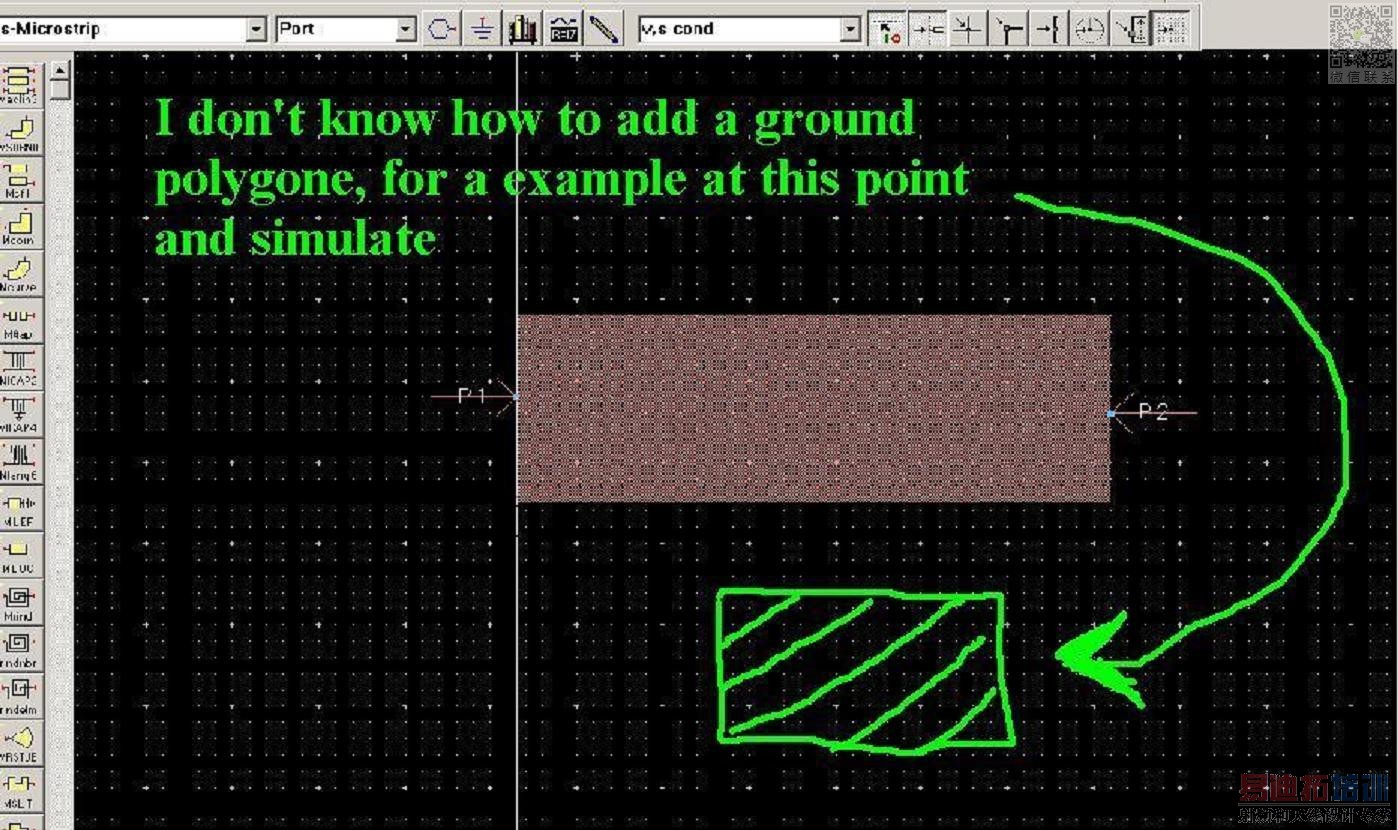
Yes, i know. I simulate my scheme with Momentum. But i don't know how to add ground polygone. Look at the picture.
You should create an extra ground shape/layer and associate a port for this layer.Then you can simulate in schematic view by grounding this port.
Thank you BigBoss for answering. But could you explain it in details? may be you have some references. I try to read a help of ADS - momentum, but i haven't undestood in full. I draw a polygon and connected a port, type of the port was reference ground. And i have an error: " Ground Reference port P3 must be associated to another" What next should i do?
Add your ground polygon on say cond2 layer and your microstrip is at cond layer, Now add ports to your micrsotrip on cond layer on edges, then add two more port just beneath previous ports on cond2 layer which will be attached to your ground,
Now go to port edditor and select the ports on cond2 layer one by one, and select the port type as ground refference and associate them to the port one above it, thats it (keep the port type on cond layer as single port)
Change the substrate accordingly and remove the ground from there,.
substrate will be like this
air
------cond
subs
-----cond2
air
Imfarhan1 . Thanks for answering. I would like to amend my question. I have to make the ground polygone on cond. If i will do as you have told, then cond2 will be ground. But i need the ground on the cond.
PS:
I want to have such structure
air
-----cond <------- here I need to have the ground polygone on this layer.
subs
-----ground
How do you intend to create the groundplane connections on the actual board? You have to do the same thing for Momentum.
Your simple illustration would have only two ports, one on each end of the microstrip line. The ground plane can then be drawn as a polygon on the same cond layer as the microstrip lines as required.
Now, assuming you are going to have through connections within the ground plane polyogon to connect to the ground conductor on the back of the board, draw 'via' structures within the ground plane polygon as required. Draw these 'vias' on a different layer, maybe hole, and then map the hole layer as a VIA to the substrate between cond and GND.
Your substrate setup should then look as follows:
Free_Space
------- -STRIP- cond
Substrate |VIA| hole
///// GND ////
Ok thats not a problem just map layer accordingly, Like the ports declayered as ground will be on cond layer, and they are reffering to ports on cond2 layer.
substrate will be like
air
---------cond2 (MS)
subs
---------cond (gnd)
air
In short just repeat whole process by swapping cond and cond2 layer.
Hope it answered your question
Thank you all. And thank you RealAEL. I have simulated my project in ADS layout and have a good result. I used the ground via for grounding microstripe lines.
I am a beginner for momentum
I have a structure in momentum
air
Cond
FR4 VIA-Hole
////GND////
I just wanted to make sure if i use the viagnd structure it will link to the ground layer.
Also how does the simulator determines the size of gnd plane. I am assuming it lays it to cover entire strucure above?
Thanks
@sajan09
Any layer maped as via acts as via it can be other than via, hole. diel etc
but make sure what ever layer you map as a via should have a structure in layout. let me explain
if you want to add a via between cond layer and ground
make your strip on cond layer
make a polygon on anyother layer say hole
now go to material editor and define it like this
cond
------hole
GND
second part
For predefined GND the momentum considers the infinite ground plane NOT only underneath the design so if you need only under you design you have to define it by your self
hope that answered you question
@sajan09
The gnd when connected using through holes(vias) act as gnd.
In momentum the Gnd specified is considered as a infinite gnd plane. If u want to have a realistic scenerio u can use box structure.
Thanks for your replies
The question I now have is
If i have to model a 2 layer PCB. Top layer for signal routung and bottom layer ground. Can I use momentum structure
cond
diel VIA(hole)
/////GND////
or i should do
cond
diel VIA(hole)
cond2
and then attach ground reference ports on the cond2 layer
Well, if u have continous gnd(w/o discontinuities) without in the 2nd layer u can go with the first approach.
hi ...i have to model a 3 layer PCB.....my layers should be in the following way....
free space
cond1(micro strip)
substrate
ground
substrate
cond2(microstrip)
free space
how to model this in ADS momentum and i also want coupling between cond1 and cond2 .....how to define the layers.....
Hello all!
I have a question:if I only need a single layer,which means there's no GND on layer 2,I just have microstrip and GND on same layer,to avoid floating the GND,I can connect the GND of this module to the board through RFcable.Then how can I set the momentum?
Best regards!
申明:网友回复良莠不齐,仅供参考。如需专业帮助,请学习易迪拓培训专家讲授的ADS视频培训课程。
上一篇:X Band transreciever module using ads
下一篇:adding box in ADS momentum
ADS培训课程推荐详情>>
 国内最全面、最专业的Agilent ADS培训课程,可以帮助您从零开始,全面系统学习ADS设计应用【More..】
- Agilent ADS教学培训课程套装
- 两周学会ADS2011、ADS2013视频教程
- ADS2012、ADS2013射频电路设计详解
- ADS高低阻抗线微带滤波器设计培训教程
- ADS混频器仿真分析实例视频培训课程
- ADS Momentum电磁仿真设计视频课程
- ADS射频电路与通信系统设计高级培训
- ADS Layout和电磁仿真设计培训视频
- ADS Workspace and Simulators Training Course
- ADS Circuit Simulation Training Course
- ADS Layout and EM Simulation Training Course
- Agilent ADS 内部原版培训教材合集