- 易迪拓培训,专注于微波、射频、天线设计工程师的培养
Microwave Office CPW EM-Simulation
I've recently had to migrate from ADS to Microwave office, and I'm trying to figure out some of the basics with the EM simulation tools. I've had success with microstrip lines, both 3D and 2.5 D simulators. However, when i try to model CPW lines, I begin to run into an issue. As the software suggests, I was able to model some CPW structures using the EMSight.
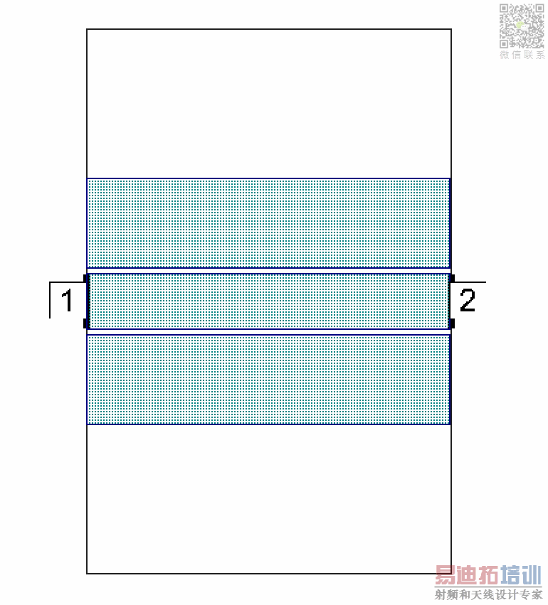
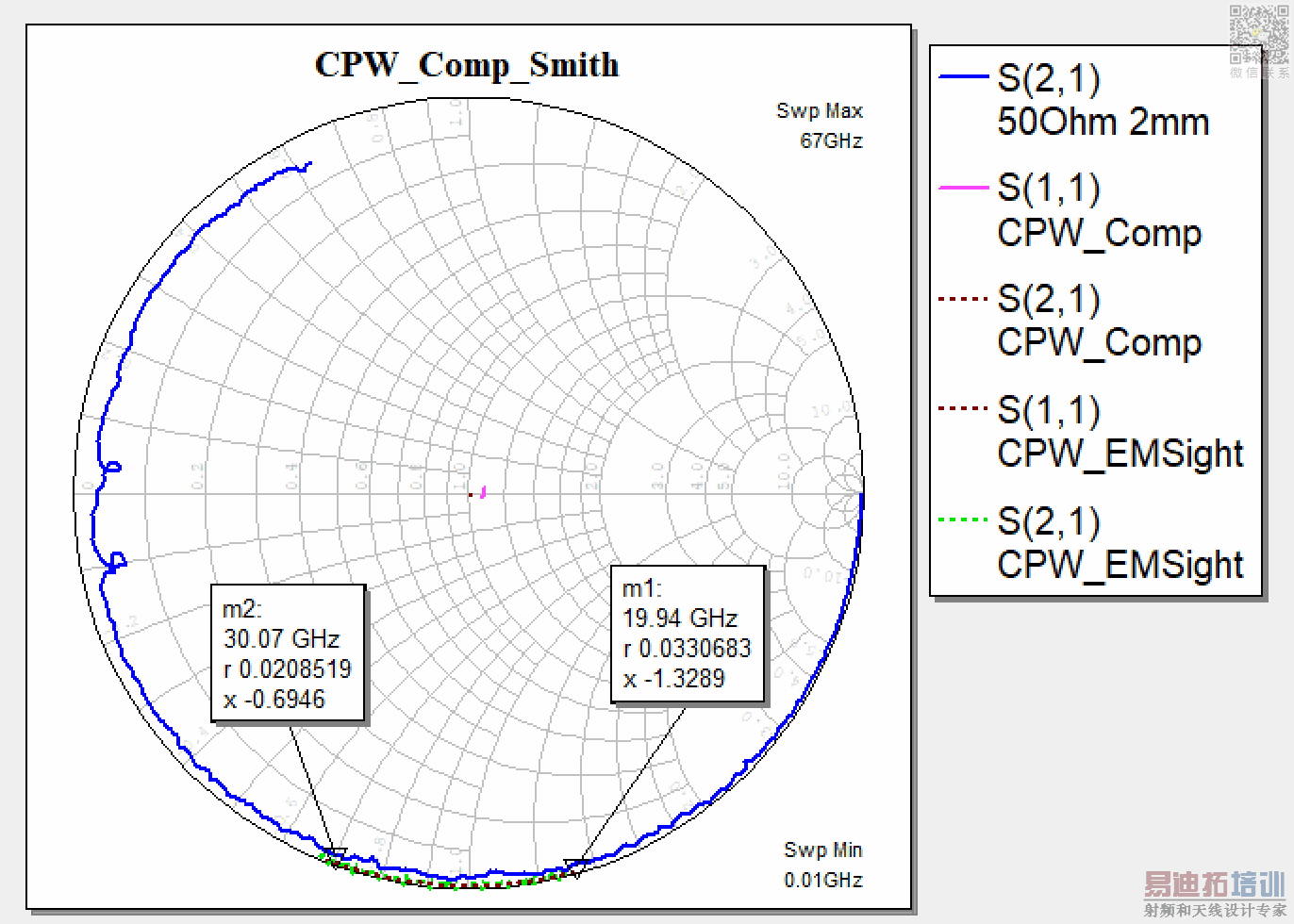
I created the simplest model possible. The stack up is one dielectric layer (not included the air) , one metal layer, and a copper ground plane. Using some dimensions from TxLine, i created a 50 Ohm line and the simulator had no issues. I created a circuit schematic to compare the EM results to an actual measured line, and a circuit model using the CPW closed form model in microwave office.
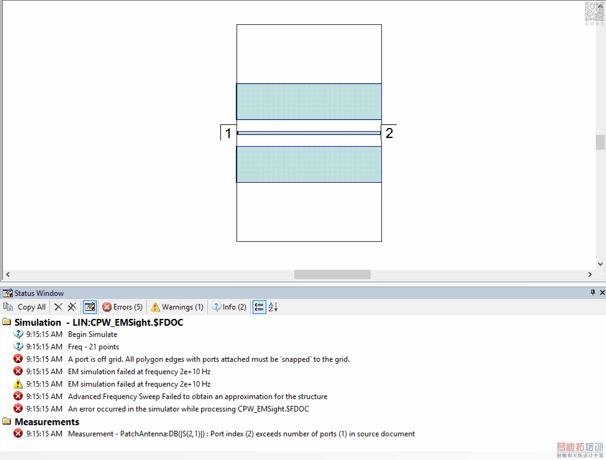
The simulated results don't match the loss of the measured line correctly, but I can be sure the EM simulation is giving me reasonable results. I run into a problem when I try and change the line geometry to a high impedance line. I changed nothing about the model setup, but i reduced the center line thickness to try and model a ~150 Ohm line, I begin to run into problems.
I've tried scouring the net for solutions to the errors i get (shown at the bottom of the figure above). I am having no luck. Any advice would be much appreciated.
Thanks in advance,
Sami
There are errors..
-Where the VIAS just besides/around the Microstrip Line ?There must be VIAS on both sides to implement CPWG.
-If you have transferred this structure from ADS, there are some off-grid errors ( see. log messages ), correct them.Increase the box size and replace the Ports accordingly..
-AWR EMSight is a grid based EM simulator not like ADS Momentum, so Ports,metallic structures,Vias etc. have to be on-grid.
-Axiem is newer EM simulator of AWR, try with it..
If it's possible, post your project file here..let me check it deeper..
You ain't kidding.
All my initial work induced vias. For fun, i tried a few simulations without, and I got the same results. So in these initial trials, i wanted to keep it as simple as possible. Also, a lot of my issues were in the grid size, meshing, etc....
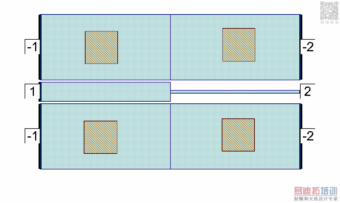
After some more scouring on the internet and on the ARW website I came across some great resources. Good lesson for not throwing in the towel too early. Turns out the best method for this is the Axiem solver, however, I was initially setting up my ports all wrong. For CPW, the ports in the Axiem have to be driven deferentially (fun times including negative port numbers). Those port definitions help to force the explicit ground reference.
I not saying all this to toot my own horn, but in case someone else searches for a solution
Thanks for the reply!
Having some large vias somewhere (outside the meaningful current path) as shown in your screenshot should not have much effect anyway.
Vias: the conducting side walls in EMSight will create a connection between side grounds and bottom ground - if the side grounds just touch the side wall without using a port there.
For GCPW with both side grounds and bottom ground, be careful with negative port number on the side grounds. You would then have a differential excitation of the top layer with the +/- ports, with the bottom ground (touching the side wall) at mid potential. That's not realistic if your PCB has vias connecting all the grounds.
AWR Microwave Office 培训课程套装,视频教学,帮助您快速学习掌握MWO...
上一篇:哪位好心能分享下AWR2010版本的软件
下一篇:AWR V11 下载


