- 易迪拓培训,专注于微波、射频、天线设计工程师的培养
MWO仿真功分板提示的错误
录入:edatop.com 点击:
大家好!
今天在仿真功分板,大家知道,功分板是有很多拐弯的地方,那么对应MWO里面什么样的Bends呢?
我看有 Microstrip-----Bends ; Stripline-----Bends ;我的功分板是微带线形式的,是不是应该选前者?
另外,在用Microstrip-----Bends 里的 MBENDA 后,仿真显示: (W/H) strongly Recommend<=2 ?
为什么宽度和厚度比值要小于等于2,这我就不理解了,假设所用PCB板材的厚度是1mm,那岂不是规定带线的宽度不能能超过2mm
? 这是什么原因呢?
望高手予以解答!急切期待!
今天在仿真功分板,大家知道,功分板是有很多拐弯的地方,那么对应MWO里面什么样的Bends呢?
我看有 Microstrip-----Bends ; Stripline-----Bends ;我的功分板是微带线形式的,是不是应该选前者?
另外,在用Microstrip-----Bends 里的 MBENDA 后,仿真显示: (W/H) strongly Recommend<=2 ?
为什么宽度和厚度比值要小于等于2,这我就不理解了,假设所用PCB板材的厚度是1mm,那岂不是规定带线的宽度不能能超过2mm
? 这是什么原因呢?
望高手予以解答!急切期待!
楼主对板材之类的可能不太了解吧 多差些资料看看就懂啦 微带传输线一般是Microstrip
仿真显示: (W/H) strongly Recommend<=2 ? ?@@BIg-
怎么解释?
按照帮助文档的要求W/H应该大于等于0.25。
至于上限没有给出,楼主遇到的提示和奇怪,请给出截图,或者相应工程。
This circuit component models an optimum Miter of an arbitrary angled bend in the Microstrip signal conductor. The model assumes a Quasi TEM mode of propagation matched to a Microstrip line of width (W) and incorporates the effects of dielectric and conductive losses. The basis of the model is a curve fit of experimentally determined optimum miters at specific angles within the specified range. At this time, the optimal miter percentage must be interpolated from the following table.
The parameter MSUB specifies the Microstrip Substrate element, which defines additional cross sectional parameters of the transmission line. M = 100 (x/d) 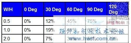
楼主设计功分器,建议参考例子文档
4_way_power_splitter
多研究自带例子很有好处 哈
AWR Microwave Office 培训课程套装,视频教学,帮助您快速学习掌握MWO...
上一篇:Microwave Office Training Introduction to EM Simulation 55页 ppt 格式
下一篇:上变频器的设计
