- 易迪拓培训,专注于微波、射频、天线设计工程师的培养
HFSS15: Deembedding Parasitic Lumped Port Effects
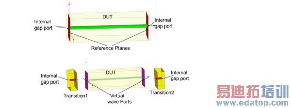
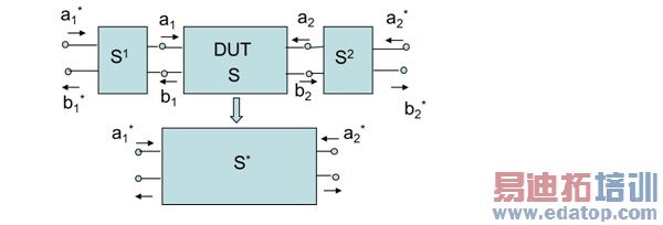
Fig. 4 shows a strip line, which is fed by internal lumped ports instead of perfect wave ports. The FEM simulation was performed using these excitations and resulted in the entire scattering matrix, S*. The goal is to calculate scattering matrix S (scattering matrix of the DUT), as if the structure were fed by perfect virtual ports. It can be done if S matrices of the transition or error boxes are known (S(1)and S(2) in Fig.2). When b* =S*a* is known and b=Sa is sought, we get:
|
| (17) |
where
are diagonal matrices:

| (18) | |
; ; ; (18)

Figure 4: Strip line (DUT) fed by two internal lumped ports

Figure 5: Black boxes of a strip line fed by two internal lumped ports
Usually, the device under test (DUT) is very large and complex. It is not possible to create perfect wave ports inside the complex geometry. However, it is not necessary to do that, when using the proposed method. The transition boxes can be independently created and solved as very small, 3D projects with two ports. In that case, the method is exact, within computational errors. In simple cases, S matrices of the transition boxes can be estimated, e.g. by a series impedance. The simplest case is when a lumped gap port is represented by a "parasitic" inductance. Applying experimental approximations for the calculation of the partial inductance of a lumped gap port ([7], [8]):
|
| (19) |
where length and w are the length and width of the gap port in millimeters, respectively. L will be in nH.
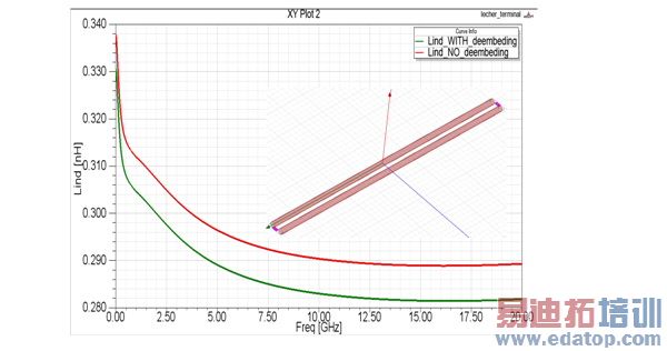
Fig. 6 shows the inductance of a pair of cylindrical wires. The two feeding lumped gap ports introduce parasitic inductances, which can be deembedded by using the above method, which analytically accounts for the DC and AC inductances. The maximum error is reduced by roughly a factor of 3; 4.3% without deembedding and 1.6% with deembedding the parasitic inductance.

Figure 6: Loop inductance of a pair of cylindrical wires with and without
deembedding the parasitic gap port inductance
Conclusions
New numerical constructs are developed for the causal modeling of transient signals in PCBs and interconnects. By introducing the correct treatment of metal traces of finite thickness, accurate DC point solution, causal material models, causal surface roughness models and deembedding parasitic effects of lumped ports, result in accurate and causal broad band frequency sweeps of S parameters. Using these techniques in a finite element code generates accurate and causal simulations provided the mesh is converged to reasonably small tolerance. The techniques described here are implemented in ANSYS HFSS. Real-life problems were solved to demonstrate the efficacy of the methods.
HFSS 学习培训课程套装,专家讲解,视频教学,帮助您全面系统地学习掌握HFSS
上一篇:Creating Smith Contour Charts
下一篇:Custom Keyboard Shortcuts


