- 易迪拓培训,专注于微波、射频、天线设计工程师的培养
EE TO PADS 转换问题
录入:edatop.com 点击:
我先是 AD的PCB 转换成 PADS 再转换成EE文件,在EE中将线画好。
然后用PADS,再导入EE画好的PCB,转换是成功,有提示转换问题,只有元件不见了,其它的还有。怎么解决!
转换提示内容如下
Expedition to PADS Layout Design and Libraries Translator (Version 9.5) 01/08/13 13:54:53
Copyright (c) 2012 Mentor Graphics Corp. - All rights reserved
------------------------------------------------------------
Input folder: D:\1\EE\PCB\EE.pcb
Output folder: EE_pads_5.pcb
[I] Preparing data...
Output file: EE_pads_5.pcb
[I] Loading...
[I] Translating Expedition design files from 'C:\Users\ADMINI~1\AppData\Local\Temp\' to PADS Layout design file
[I] Reading Pad Stacks...
[I] Reading Cells...
[I] Reading Part Numbers...
[I] Reading Job Prefernces...
[I] Reading Net Classes...
[I] Reading Net Properties...
[I] Reading Layout...
[I] Translating data...
[W] All coincident Pad Entry rules are translated to Default Rules level
[W] Discriminate Pad Entry rules found, and the rules were not translated.
[W] Route grid is not set. Primary part grid is used for setting design grid.
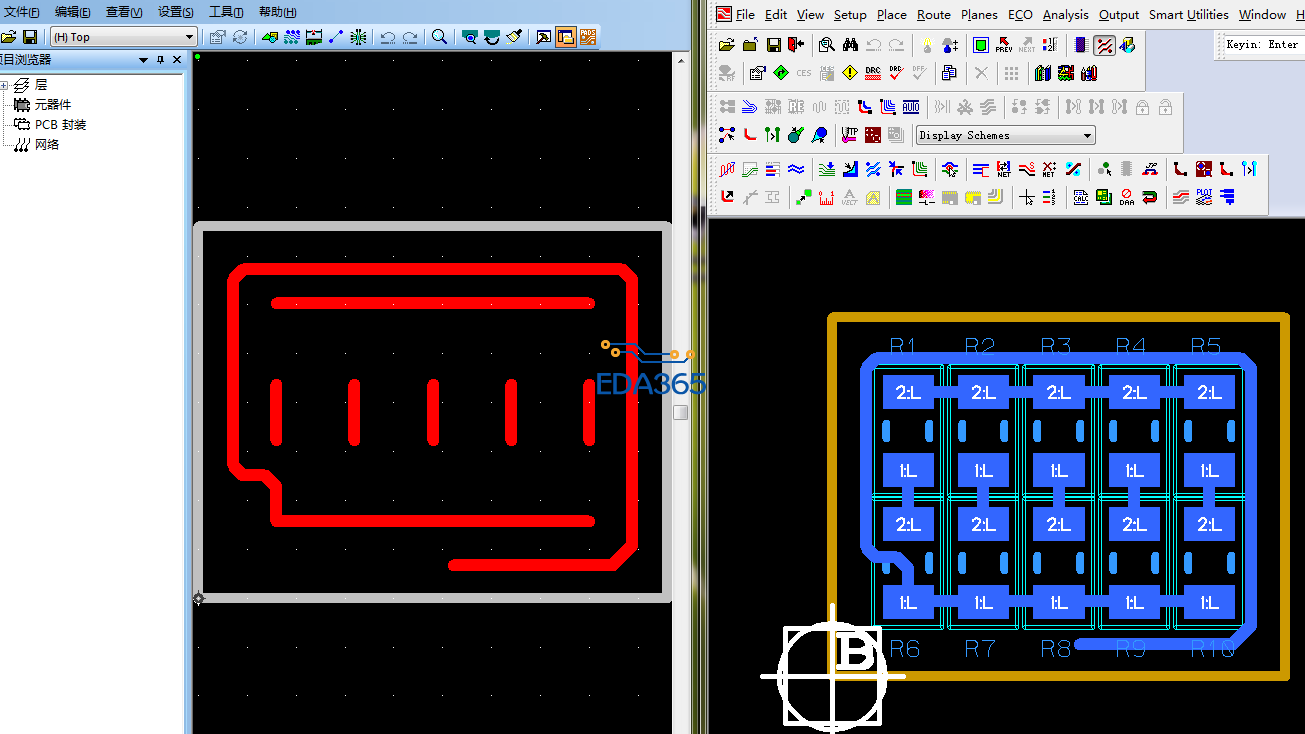
[W] Part type 'RES' is not found, and the component 'R6' was not translated.
[W] Part type 'RES' is not found, and the component 'R9' was not translated.
[W] Part type 'RES' is not found, and the component 'R10' was not translated.
[W] Part type 'RES' is not found, and the component 'R5' was not translated.
[W] Part type 'RES' is not found, and the component 'R8' was not translated.
[W] Part type 'RES' is not found, and the component 'R7' was not translated.
[W] Part type 'RES' is not found, and the component 'R4' was not translated.
[W] Part type 'RES' is not found, and the component 'R3' was not translated.
[W] Part type 'RES' is not found, and the component 'R2' was not translated.
[W] Part type 'RES' is not found, and the component 'R1' was not translated.
[W] Route outlines are not supported, and was not translated.
[W] Pin name 'R7-1' has wrong format. The pin was not included into the net 'GND'.
[W] Pin name 'R6-1' has wrong format. The pin was not included into the net 'GND'.
[W] Pin name 'R8-1' has wrong format. The pin was not included into the net 'GND'.
[W] Pin name 'R9-1' has wrong format. The pin was not included into the net 'GND'.
[W] Pin name 'R10-1' has wrong format. The pin was not included into the net 'GND'.
[W] Net 'GND' don't have properly pin pair. Vias of the net were not translated and traces were translated to open coppers.
[W] Pin name 'R1-1' has wrong format. The pin was not included into the net 'NETR1_1'.
[W] Pin name 'R6-2' has wrong format. The pin was not included into the net 'NETR1_1'.
[W] Net 'NETR1_1' don't have properly pin pair. Vias of the net were not translated and traces were translated to open coppers.
[W] Pin name 'R2-1' has wrong format. The pin was not included into the net 'NETR2_1'.
[W] Pin name 'R7-2' has wrong format. The pin was not included into the net 'NETR2_1'.
[W] Net 'NETR2_1' don't have properly pin pair. Vias of the net were not translated and traces were translated to open coppers.
[W] Pin name 'R3-1' has wrong format. The pin was not included into the net 'NETR3_1'.
[W] Pin name 'R8-2' has wrong format. The pin was not included into the net 'NETR3_1'.
[W] Net 'NETR3_1' don't have properly pin pair. Vias of the net were not translated and traces were translated to open coppers.
[W] Pin name 'R4-1' has wrong format. The pin was not included into the net 'NETR4_1'.
[W] Pin name 'R9-2' has wrong format. The pin was not included into the net 'NETR4_1'.
[W] Net 'NETR4_1' don't have properly pin pair. Vias of the net were not translated and traces were translated to open coppers.
[W] Pin name 'R5-1' has wrong format. The pin was not included into the net 'NETR5_1'.
[W] Pin name 'R10-2' has wrong format. The pin was not included into the net 'NETR5_1'.
[W] Net 'NETR5_1' don't have properly pin pair. Vias of the net were not translated and traces were translated to open coppers.
[W] Pin name 'R2-2' has wrong format. The pin was not included into the net 'VCC'.
[W] Pin name 'R1-2' has wrong format. The pin was not included into the net 'VCC'.
[W] Pin name 'R3-2' has wrong format. The pin was not included into the net 'VCC'.
[W] Pin name 'R4-2' has wrong format. The pin was not included into the net 'VCC'.
[W] Pin name 'R5-2' has wrong format. The pin was not included into the net 'VCC'.
[W] Net 'VCC' don't have properly pin pair. Vias of the net were not translated and traces were translated to open coppers.
[I] Completed
然后用PADS,再导入EE画好的PCB,转换是成功,有提示转换问题,只有元件不见了,其它的还有。怎么解决!
转换提示内容如下
Expedition to PADS Layout Design and Libraries Translator (Version 9.5) 01/08/13 13:54:53
Copyright (c) 2012 Mentor Graphics Corp. - All rights reserved
------------------------------------------------------------
Input folder: D:\1\EE\PCB\EE.pcb
Output folder: EE_pads_5.pcb
[I] Preparing data...
Output file: EE_pads_5.pcb
[I] Loading...
[I] Translating Expedition design files from 'C:\Users\ADMINI~1\AppData\Local\Temp\' to PADS Layout design file
[I] Reading Pad Stacks...
[I] Reading Cells...
[I] Reading Part Numbers...
[I] Reading Job Prefernces...
[I] Reading Net Classes...
[I] Reading Net Properties...
[I] Reading Layout...
[I] Translating data...
[W] All coincident Pad Entry rules are translated to Default Rules level
[W] Discriminate Pad Entry rules found, and the rules were not translated.
[W] Route grid is not set. Primary part grid is used for setting design grid.
[W] Part type 'RES' is not found, and the component 'R6' was not translated.
[W] Part type 'RES' is not found, and the component 'R9' was not translated.
[W] Part type 'RES' is not found, and the component 'R10' was not translated.
[W] Part type 'RES' is not found, and the component 'R5' was not translated.
[W] Part type 'RES' is not found, and the component 'R8' was not translated.
[W] Part type 'RES' is not found, and the component 'R7' was not translated.
[W] Part type 'RES' is not found, and the component 'R4' was not translated.
[W] Part type 'RES' is not found, and the component 'R3' was not translated.
[W] Part type 'RES' is not found, and the component 'R2' was not translated.
[W] Part type 'RES' is not found, and the component 'R1' was not translated.
[W] Route outlines are not supported, and was not translated.
[W] Pin name 'R7-1' has wrong format. The pin was not included into the net 'GND'.
[W] Pin name 'R6-1' has wrong format. The pin was not included into the net 'GND'.
[W] Pin name 'R8-1' has wrong format. The pin was not included into the net 'GND'.
[W] Pin name 'R9-1' has wrong format. The pin was not included into the net 'GND'.
[W] Pin name 'R10-1' has wrong format. The pin was not included into the net 'GND'.
[W] Net 'GND' don't have properly pin pair. Vias of the net were not translated and traces were translated to open coppers.
[W] Pin name 'R1-1' has wrong format. The pin was not included into the net 'NETR1_1'.
[W] Pin name 'R6-2' has wrong format. The pin was not included into the net 'NETR1_1'.
[W] Net 'NETR1_1' don't have properly pin pair. Vias of the net were not translated and traces were translated to open coppers.
[W] Pin name 'R2-1' has wrong format. The pin was not included into the net 'NETR2_1'.
[W] Pin name 'R7-2' has wrong format. The pin was not included into the net 'NETR2_1'.
[W] Net 'NETR2_1' don't have properly pin pair. Vias of the net were not translated and traces were translated to open coppers.
[W] Pin name 'R3-1' has wrong format. The pin was not included into the net 'NETR3_1'.
[W] Pin name 'R8-2' has wrong format. The pin was not included into the net 'NETR3_1'.
[W] Net 'NETR3_1' don't have properly pin pair. Vias of the net were not translated and traces were translated to open coppers.
[W] Pin name 'R4-1' has wrong format. The pin was not included into the net 'NETR4_1'.
[W] Pin name 'R9-2' has wrong format. The pin was not included into the net 'NETR4_1'.
[W] Net 'NETR4_1' don't have properly pin pair. Vias of the net were not translated and traces were translated to open coppers.
[W] Pin name 'R5-1' has wrong format. The pin was not included into the net 'NETR5_1'.
[W] Pin name 'R10-2' has wrong format. The pin was not included into the net 'NETR5_1'.
[W] Net 'NETR5_1' don't have properly pin pair. Vias of the net were not translated and traces were translated to open coppers.
[W] Pin name 'R2-2' has wrong format. The pin was not included into the net 'VCC'.
[W] Pin name 'R1-2' has wrong format. The pin was not included into the net 'VCC'.
[W] Pin name 'R3-2' has wrong format. The pin was not included into the net 'VCC'.
[W] Pin name 'R4-2' has wrong format. The pin was not included into the net 'VCC'.
[W] Pin name 'R5-2' has wrong format. The pin was not included into the net 'VCC'.
[W] Net 'VCC' don't have properly pin pair. Vias of the net were not translated and traces were translated to open coppers.
[I] Completed
为什么要转,你不是两个工具都会用么
有些工程,比如AD的,或者PADS的,工程可能已经做了一部分,或者修改比较多,想转入EE中再重新布线。完成后,再转回PADS或者AD中,为一个完整的工程。
我在转换时遇到icdb出错 请问小编是怎么设置的?、
把CES关闭再转试一试。
呵呵,如果EE不能转PADS,比如导入错误,那么关闭CES后,的确就可以导入了。这个方法我知道。
我想知道的是,PADS转EE的文件,如果开启CES后,是不能导入的,但关闭后,虽然能导入,但就如我所问的问题一样,没有元件封装的。其它的可以转换
软件之间的转换不可能十分完美,由于没有看到实际情况,不太清楚造成所述问题的原因所在,但目前的解决方法可以保留转换后工程的线,铜皮孔等需要的信息,拷贝到没有问题的PADS工程上.由于本人能力有限,不知道这样的方法是否可以帮助您解决问题
呵呵,这样的解决方案貌似不好。
我说一下具体过程吧。
1,不管用什么软件生成网络表,或者用原生的DX, 然后在EE中做的PCB工程。基本可以完美导入PADS中。
2,如果你是AD转PADS转EE,或者PADS转EE,你再想从EE转回PADS,问题就来了,如果打开了CES,要关闭CES才能导入PADS,虽然能导入了,但是,元件却不见了,就像我顶楼所贴的提示内容差不多。
我想解决的是2过程。
因为有些工程可能原来是AD的,或者PADS,这样可以在EE中布局布线,完成后,再导回PADS,这样就是一个完整的工程。
请问下,EE怎么转PADS?
谢谢!
规则都导进去了吗?
CES没打开,在PADS里面import出现iCDB无法打开的错误
Cadence Allegro 培训套装,视频教学,直观易学
上一篇:求教mentor模块复用操作步骤
下一篇:EE2005如何设置通孔优先?