- 易迪拓培训,专注于微波、射频、天线设计工程师的培养
allegro叠层设置中shield一栏的作用是什么?
录入:edatop.com 点击:
 这个shield栏,我点与不点,我尝试了,对操作没有什么不同啊,求解
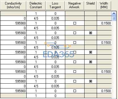
自己顶一下,大家来探讨下,这个shield选项只有在plane层才有
我这是16.5版本
没人 知道吗,我看了allegro的help文档,也没说是干啥用的
崇拜英文好的牛人,我至今看不懂英文的help文件
我也想知道!
就这个还没人解答啊,看来我这小菜鸟要努力啊
Shield : (in the stackup editor) If shield option is not checked, Allegro PCB SI accept planes are not ideal or solid and have multiple planes and it forces to find effects plane boundaries.
原文如下:
Allegro PCB SI can deal with splits or slot, void problems. Using "shield" and "ANL_MIN_VOID_AREA" Properties, you can see effects because of impedance discontinuity.
Shield : (in the stackup editor) If shield option is not checked, Allegro PCB SI accept planes are not ideal or solid and have multiple planes and it forces to find effects plane boundaries.
ANL_MIN_VOID_AREA : (minimum void area) For void or slot it is useful. Allegro calculate void effects in power layers via transtion. (Via perforations) You can find "ANL_MIN_VOID_AREA" property in the User references --> Signal Analysis section. Maybe you must play "Geometry Window" and "min coupled length".
In my some design, I have to route transmission lines over the voids, slots and near edge of power plane.I saw Impedance changing. For example, In slots or void Allegro add high impedance ransmission line according to other transmission lines. In split planes you know adding capacitor where you are rossing the split will give more realistic result.
之前就听说allegro能考虑跨分割的阻抗变化,但是一直都不知道在哪里设置,现在终于明白了
我是在pcb editor那个叠层设置里面右下方看的help文档,没看到这段文字, 请问你这段文字是在哪里的help文档? 另外,这个shield设置是与si 仿真有关是吧,与pcb editor无关是吧
这个应该是仿真时候用的。勾选了的话就认为是无限大金属平面,仿真的时候计算比较方便。不勾选就要考虑边缘效应之类的影响。出版图应该没影响的。
谢谢,对PCB SI了解太少,那些SI牛人 都离我们太遥远! 能指导一下我吗,朋友QQ932026701
根据上面那段E文的意思大概应该是,shield勾上就表示理想平面,不勾就表示按实际的来。
都是牛人啊,我都没关注过这些
请问各位师傅们ALLEGRO16.3叠层怎么增加呀?我怎么增加不了,在此谢过好心人