- 易迪拓培训,专注于微波、射频、天线设计工程师的培养
spb16.6 apd Via Shape Shorting 功能能用吗?
录入:edatop.com 点击:
What's Good About APD’s Shape Shorting? You’ll Need the 16.6 Release to See!
By Gerald "Jerry" Grzenia on November 13, 2012
Comments(0)
Filed under: PCB design, via, advanced package designer, APD, IC Packaging and SiP Design, IC Packaging, PCB, layer stacks, Digital SiP design, design, High Speed, blind vias, packaging, Allegro Package Designer, IC/package co-design, inset vias, vias, Allegro GUI, Grzenia, Allegro 16.6, shorting vias, shape shorting
In some designsflows, you need to connect two plane shapes on the same net, but on different layers, together with vias in order to improve connectivity. These “shorting” vias are placed in a regular pattern across the overlapping areas of the shape, in such a way as not to interfere with any routing on layers between the two shapes.
The 16.6 Allegro Package Designer (APD) product now provides a mechanism for constructing these arrays of shape-to-shape shorting via arrays, deleting them, and updating them as the design progresses.
Read on for more details …
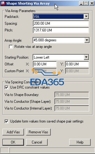
You first select the two shapes to be shorted together. This will update the form fields to restrict the padstacks available, and, if parameters already exist for this shape pairing, will optionally load the existing via array values. You can customize any fields as necessary on the form, and finally presses the “Add Vias” or “Remove Vias” button to perform the desired operation.
Note: If the two selected shapes already have a via array between them, it will be cleared before generating a new array.
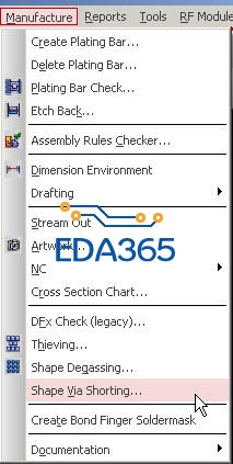
Manufacture > Shape Via Shorting:
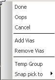
The RMB popup menu, shown below, contains the standard Done, Oops, and Cancel items.
As well as entries for add vias and for remove vias:
•adstack: This will list only those via padstacks applicable for the currently selected shapes. For instance, when the command is first started (no shapes selected), it will show all via padstacks in the design. When you select the first shape, the list gets trimmed to just those that start or end on the specified layer. When the second shape is selected, it is fully restricted to only those padstacks going between those two specific layers. At any time, if the current selection becomes invalid for the selected shapes, the tool will change to the first padstack alphabetically.
•Spacing: The airgap between vias in the via array. This is derived from the current selected via padstack and pitch. You should ensure this value is at least equal to your via to via DRC constraint value for the constraint set this net belongs to. This defaults to the via to via DRC spacing constraint on the top layer of the design.
•itch: The center to center distance between vias in the shorting via array. This is tied to the spacing value above, and changing one will change the other.
•Array Angle: The angle at which the array will be created. A 0-degree angle means all the vias are placed in horizontal rows / vertical columns like a standard grid. Adding an array angle is useful is the shape is primarily at an angle (think like the spokes of a wheel). The default value will be 0 degrees.
•Rotate Vias at Array Angle: If you specify an angle for the array above, and the padstack definition consists of any non-circular pads, drill holes, etc., you may wish to have the vias instantiated with a rotation that matches the array angle to maintain consistent separation. This option allows you to do that.
•Starting Position: Where the reference point for the via array is. Choices are upper left/right, lower left/right, and custom point. The corner selections are relative to the reference shape’s extents box.
•Offset X / Y: The offset X and Y values relative to the indicated starting position. For example, an X offset of 50um from the upper left corner will have a “legal” via array position 50 microns to the right of the top-left corner of the reference shape’s extents box. The array will extend from this point in all directions, at the pitch and angle specified, to cover the entire shape region.
•Custom Point X/Y: If the starting position is “Custom Point”, these fields are enabled, and allow you to specify an absolute database position to use as the via array’s reference position. This is particularly useful if one needs to offset via arrays between different layer pairings, or if multiple via arrays connect to a single plane shape.
•Use DRC Constraint Values: If enabled, this will cause the tool to pull the required spacing constraints from the DRC constraint system for the database. Thus, different values can be had on each internal layer, on each shape’s layer, and in constraint regions. Defaults to on.
•Via to Shape Boundary: If not using the DRC system’s constraint values, you may enter a value for the vias to clear the two shorted plane shapes’ outlines. This defaults to the via to shape spacing on the top layer of the design if enabled.
•Via to Conductor (Shape Layers): If not using the DRC system’s constraint values, you may enter a value for the vias to clear other routing objects (pins, vias, clines, etc) on the same layers as the shapes being connected. This defaults to the via to cline spacing on the top layer of the design if enabled.
•Via to Conductor (Internal Layers): If not using the DRC system’s constraint values, you may enter a value for the vias to clear routing objects (pins, vias, clines, shapes, etc) on all routing layers BETWEEN the layers the shapes being connected are on. This defaults to the via to cline spacing on the top layer of the design if enabled.
•Update Form Values from Saved Shape Pair Settings: This option defaults to on. When a shorting via array is created between two shapes, the tool will store the array’s parameters in the database. When these two shapes are next selected (and this option is enabled), the stored parameters will be updated to the form. This will include the values for all fields from the padstack through to the via to conductor spacing settings.
•Add Vias: Add shorting array of vias between the two selected shapes. If shorting vias between these shapes already exist, they will first be removed. This will prevent duplicate vias in the database.
•Remove Vias: If only a single (reference) shape is selected, this will remove all shorting via arrays between this shape and any other shape. If two shapes are selected, this will remove only those vias that connect specifically between the two selected shapes.
Example
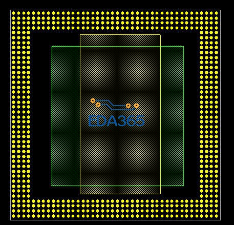
Below we have a substrate with GND planes on the Surface and Base layers that we would like to connect with seed vias:
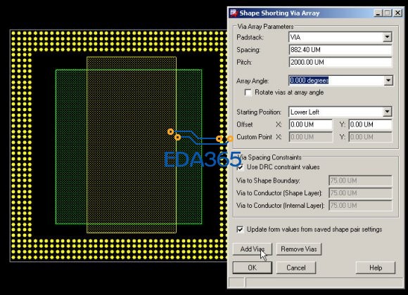
We bring up the Shape Shorting Via Array tool and set it as needed. Select the two shapes to be shorted on the work surface and then select the Add Vias button:
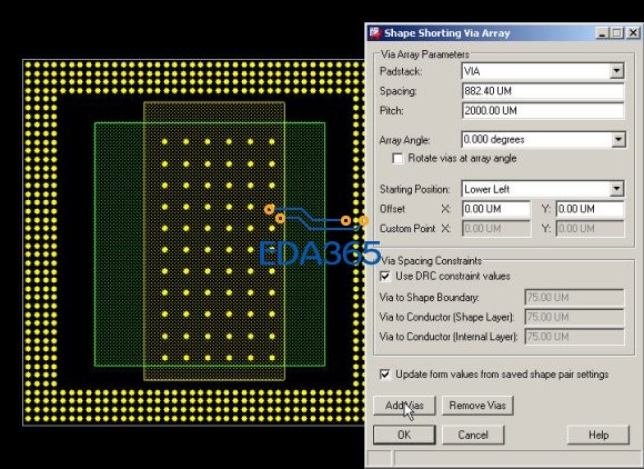
The shapes are now shorted together per our settings:
Please share your experience using this new capability!
