- 易迪拓培训,专注于微波、射频、天线设计工程师的培养
Are ideal waveguide port and coaxial feed same in CST?
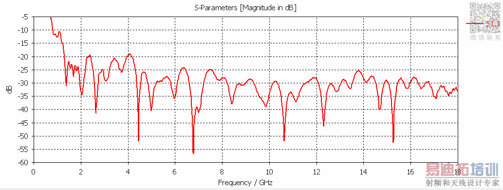
i'm designing a double-ridged horn antenna in CST. First, i designed it with an ideal waveguide port(i chose back surface of the waveguide and add waveguide port) and i took very good s11 and farfield radiation results in my working band(<-20 dB from 1 to 18 GHz and good directivity in the direction of radiation).
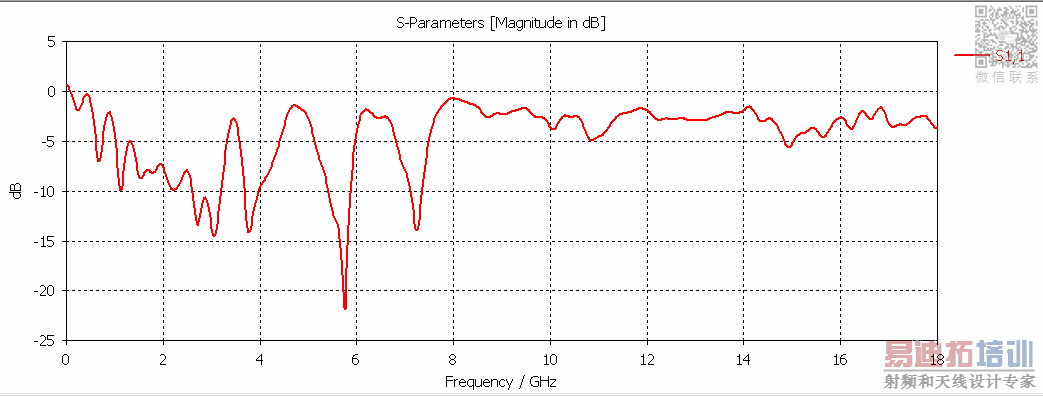
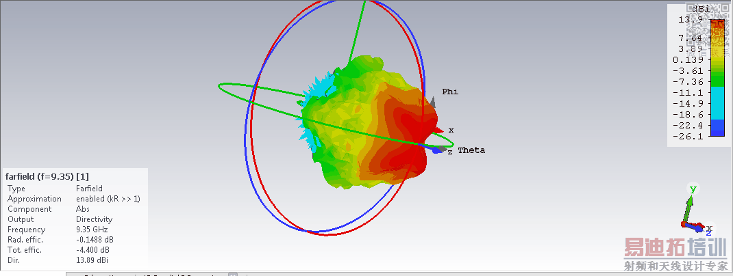
But when i feed the antenna with a coaxial probe from bottom of the waveguide, my whole s11 results are corrupted. They are below -10 dB in lots of band i simulate and in radiation patterns main lobs are divided and there are so much side lobs.
I checked some journals and youtube videos and i saw when people add coaxial probe to a horn antenna their s-parameters also corrupted.
- So, I want to ask that these corruptions are normal? if they are not can you advice me what can i do to fix these ? I changed the position of probe. that's not affect so much.
- Also I want to ask which one gives me the more realistic results for horn antenna - ideal waveguide port or coaxial probe. It seems I'll produce this antenna with coaxial probe.
Thank you.
there is a transition for signal from waveguide to coaxial once coaxial is added to waveguide. so a proper transition is required to design to get a good match. Have a look at this link for transition design - https://www.microwaves101.com/encycl...ax-transitions
Such transition are commercially available. waveguide size for different frequency band follow some standard to be able to use with the commercial transition. with this in view horn antenna designer fix their feed end of horn antenna similar to standard size. this way the designed antenna can be practically used in any system with standard transition and in simulation one can use just the waveguide port to measure the antenna performance.
First i want to specify I wrote wrong the part of "They are below -10 dB" it must be "They are above -10dB".
i tried many of ways to solve this problem but i couldn't. I changed the position of the feed, height of the pin, changing radius of the pin, teflon and outer cover(copper), changing materials of the pin, dielectric(teflon) and outer copper of the feed, also I add cavity back but nothing has happened so far. It's not working. As I see i'm doing everything properly but I don't know why it's not working. Can somebody help me ?
Also I can send the .cst file of the design if someone may check. I would be so appreciate...
Thanks again...
Sorry for second reply but I really need help.
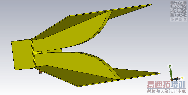
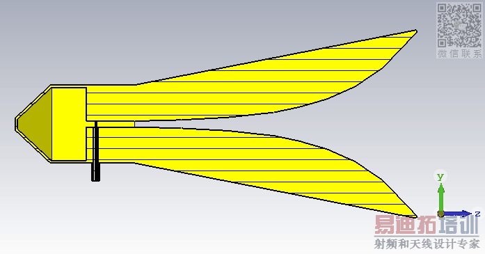
For a more detailed view I want to add some screenshots;
By the way i had to decrease cells because my computer is not so good and I had to speed up the calculation but I don't think this makes results this much bad.
S11 when I used ideal waveguide port; (Cells per wavelength - near to model : 9)
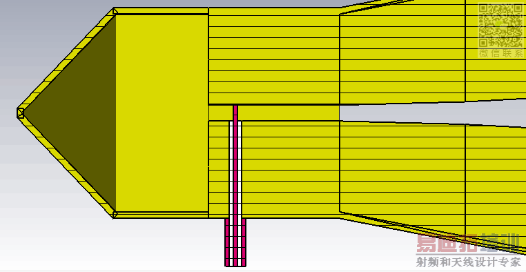
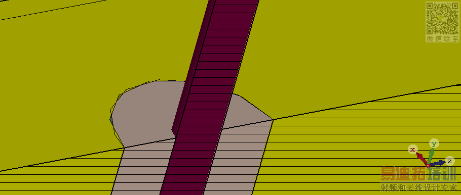
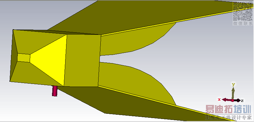
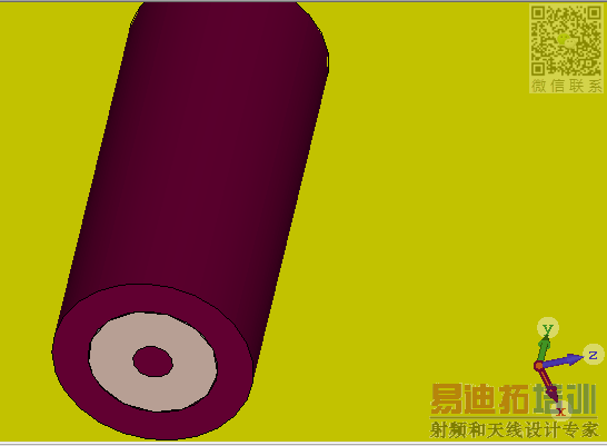
Antenna feed part with coaxial feed;
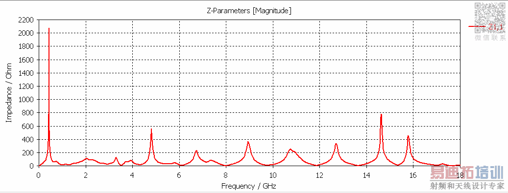
S11 with coaxial feed; (Cells per wavelength - near to model : 3)
Have a look at existing coax to waveguide transitions (post #2 above), they have a flat end section. No cone.
in double-ridged waveguides there is a method which called "cavity back". That cone ending is coming from there. I also tried flat end but it's not working.
I just see this now - this cannot work. You should keep a minimum of 10 cells per wavelength to properly resolve the fields. With 3 cells/wavelength, the field is undersampled and you cannot get any useful results.
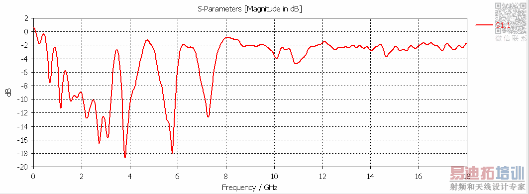
same coaxial feed structure with 10 mesh ;
i think problem is not about that.
Please post more pics of your design .. from different angles... to have better insight into the design.
from the pic posted it appears that the probe is connected to upper ridge as well.. is it so? if its so then it should not be like that.
also its difficult to figure out what is the cone part with different color implies
keep the number of mesh per wavelength more than 10, use 20... less than 10 result can not be trusted
I added more pics and cst(2018) file of my design in the link below.
(Moderator action: removed link to external server. Faild to load pictures, anyway)
Results are taken from 10 mesh calculation.
Thank you.
Link was deleted. I'm adding some pics here
1) As I see in the articles the connection must be like this.
2) I added more pics
3) I simulated it with 15 also but nothing has changed.
Thank you.
then I can suggest to focus on transition part first without tapered ridge part.
optimize with pin position, thickness, ridge gap and cavity dimension...
check page 227 of http://citeseerx.ist.psu.edu/viewdoc...=rep1&type=pdf
申明:网友回复良莠不齐,仅供参考。如需专业解答,请学习易迪拓培训专家讲授的CST视频培训教程。
上一篇:[How] Import CST MWS Mesh settings into HFSS Simulator
下一篇:Using sensitivity analysis in CST

