- 易迪拓培训,专注于微波、射频、天线设计工程师的培养
PCB and schematic simulation for CE with CST
录入:edatop.com 点击:
Hi guy,
i'm currently doing pcb simulation with CST. i have some basic question to ask here.
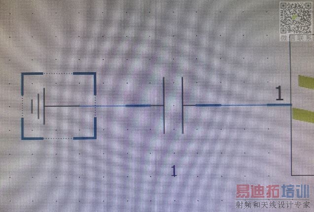
let say i assign a discrete port in my PCB for a series component as shown in figure below
In schematic tab i assign this discrete port as lump component. the connection is shown in below. am i doing it right, by terminating the other end with a ground.
one more question if i replace it with a series resistor, i wanna probe the signal after the series resistor, which side i should place the probe in schematic tab, the ground site or the other side?
hope someone here can answer my question.
thanks
i'm currently doing pcb simulation with CST. i have some basic question to ask here.
let say i assign a discrete port in my PCB for a series component as shown in figure below

In schematic tab i assign this discrete port as lump component. the connection is shown in below. am i doing it right, by terminating the other end with a ground.
one more question if i replace it with a series resistor, i wanna probe the signal after the series resistor, which side i should place the probe in schematic tab, the ground site or the other side?
hope someone here can answer my question.
thanks
Yes, that creates a connection from the ports plus terminal to the ports local reference.
If your port represents a series element, then both is wrong. You need to probe voltage against the "global" ground where the input ports refer to. Which means you need another port that has ground reference connected to that global ground.
sorry u mean if it reprensent a series element then i cant place ground on the other side on the schematic tab?
申明:网友回复良莠不齐,仅供参考。如需专业解答,请学习易迪拓培训专家讲授的CST视频培训教程。
上一篇:Simulation of a RFID tag antenna with CSt MWS
下一篇:SAR calculation in CST 2014 , after simualting SAR when i wanna see 3d result ......