- 易迪拓培训,专注于微波、射频、天线设计工程师的培养
CST simulation for grounded CPW
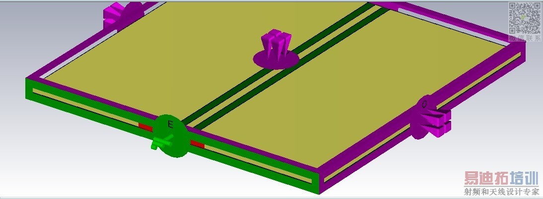
If the port is in boundary plane (shown in fig1), port mode shows normal QTEM mode and the calculated impedance is accurate.
However, if the port is located internally, means the port is within boundary (shown in fig2), the results are totally wrong.


Boundary condition is shown in fig3.

Can anybody teach me where I'm wrong? Does it imply that waveguide port must locate in boundary plane?
BTW: Is discrete port OK to use to calculate such kind of waveguides? How to set discrete port for CPW internal port?
Thanks.
I changed CPW to Microstrip line, and this problem disappeared. Port mode and impedance calculation is no problem, no matter where I set waveguide port.
Any idea or comment is appreciated.
Discrete ports are not unsuitable for WAVEGUIDES like CPW. That's why you should use a waveguide port. From the point of definition of a waveguide port, it makes no sense to placed it somewhere inside the structure. Because how you want to excite your real cpw inside? One reason for the error could be: If you place your waveguide inside, both sides of your structure are excited. Maybe with your CPW you get strange higher order modes. For Microstrip it should work at this low frequencies.
I fully agree with what JohnJoe is saying. Even though I am new to CST, a waveguide like CPW should be feed using waveguide ports placed at the edges of your structure. And you shoud be very careful in chosing the lateral extension of your top GND planes as at very high frequencies (where lambda/2 is comparable with your top GND width) can resonate like patch antennas, and higher order modes could leak into the fundamental CPW mode.
So, the conclusin is that you should you use waveguide port excitations, placed at the edge (input and output) of your coplanar line.
Hope it helps!
PS: I can tell you that when using ports in this configuration, if proper slot/ conductor dimensions are chosen you get a 50 Ohms CPW line impedance
Thanks a lot for all your comments, guys.
After some study, I have below findings, please check them and feedback with your valuable comments.
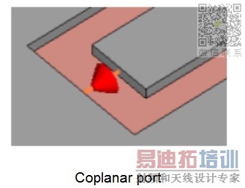
1. Discrete port for wavegudies such as microstrip and CPW is defined in CST tutorial section 'discrete port overview', as shown in fig4.

I'm not sure S-parameter calculation using such kind of discrete port is accurate or not.
I didn't see discrete port defination for grounded CPW. Maybe it implies that discrete port is not applicable for GCPW calculation.
Any comments on this?
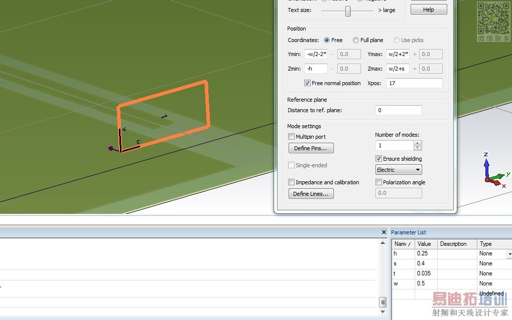
2. In CST tutorial section 'waveguide port overview', I saw 'ensuring shelding' thing for internal waveguide ports. Check below figure.

3. Using 'ensure shielding' option, waveguide port inside of structure is OK to use for GCPW. Check details in fig5.
Boudary is open for all six faces.

To first: discrete ports need to be deembed from s-paramters results. It's possible in CST with macros. But just consider the exication, the waveguide uses a TEM or QTEM mode to excite, in a case of discrete port, it's a current and, depending on discrete port setup, at one point, one face or one edge. Nevertheless it's possible to use discrete ports but not very accurate.
To second and third : agree, you can use electrical shielding but till now I don't understand the benefit of using waveguide port inside a structure in comparison with reality.
I totally agree with JohnJoe. From what I have read during last days, and having some experience other electromagnetic simulators (ADS, HFSS), discrete ports are more apropiate to microstrip like structures, they are not as precise for CPW (either without or with backside metalization). By the way, it doesn't matter wheatehr you use regular CPW or CBCPW, you should use waveguide ports. Be careful when defining their dimension as they could excite higher order modes.
With respect to 2 and 3, I still don't understand why do you want to use internal excitation! The way this circuits are probed in real life(using probe stations with pico probes placed on some CPW DC pads that are added at the extremes of your CPW structures) resembles the waveguide port excitation.
Hope that helps!
Cheers!
Both, can you describe in detail about how to do deembedding from S-parameters to get more accurate results when doing simulation with discrete ports?
BTW: I'm simulating a GCPW feed monopole antenna, and this antenna locates inside of a large PCB, this is why the CPW feedpoint is not at the boundary.
Thanks, guys.
You simulate with discrete ports and switch to the schematic screen (not model screen), from Menu -> Macros -> Construct -> Discrete Ports -> Compensate Self Inductance...
you simulate the whole pcb for the antenna? just cut it at the start of the feeding line.
Hi realfanta:
I cannot give you feedback on the deembeding of discrete ports on CST (I'm sure Johnjoe is speaking from his expeience and you should go with his suggestion) as I have not had to deal with it so far.
Regarding the need to use discrete ports as internal type ports, considering you have a well adapted 50Ohms T-line (in CPW), it should not affect the |S11| behavior, yes the phase of the reflexion coeff will be different due to obvious difference in length, but that should not alter the frequency properties (gain, directivity, radiation diagram) of your antenna. So then you could just go with the waveports placed at the boundary of your design.
In case phase variation is an issue, why don't you do as JohnJoe suggested and cut your circuit where your CBCPW feeding line starts? After that, I'm sure CST has the option of recombining the S-params of distinct blocks and obtain the final response of the whole system.
Cheers!
Thanks, both. Your suggestions really helps a lot.
I will try de-embedding of discrete ports follow Johnjoe's suggestion.
Regarding cutting PCB, I can try it and I believe it does't affect antenna gain and radiation pattern. However, I also want to see the current distribution of whole PCB, there may have unwanted current coupling from antenna structure to signal lines. This is why I simulate whole PCB. Any comments?
Thanks again.
You're welcome. One idea is to accurately characterize the antenna with waveguide ports (only the antenna), and to examine the coupling with the use of discrete ports and less accuracy on the whole pcb.
I'm simulating GCPW fed antenna but i don'n know set proper boundary condition in CST?
what is the suitable boundary condition for this structure (grounded CPW fed antenna) ?
申明:网友回复良莠不齐,仅供参考。如需专业解答,请学习易迪拓培训专家讲授的CST视频培训教程。
上一篇:[CST MW] Need help about bowtie antenna simulation in CST MW
下一篇:[Moved]Mesh generation with CST Studio

